Liquid crystal display panel

A liquid crystal display panel, glass substrate technology, applied in nonlinear optics, instruments, optics, etc., can solve problems such as end cracking, uneven brightness, light leakage, etc., to eliminate the effect of deformation and improve the effect of COGmura phenomenon

Inactive Publication Date: 2013-04-03
AU OPTRONICS (SUZHOU) CORP LTD +1
View PDF0 Cites 16 Cited by
  • Summary
  • Abstract
  • Description
  • Claims
  • Application Information

AI Technical Summary

Problems solved by technology

However, because of its weak structure, the thinner glass substrate is easily affected by local stress due to factors such as its own weight or the adhesive force of the adhesive tape in the chip-on-glass packaging process, and the glass substrate and the chip have different thermal expansion. The cold shrinkage factor causes the glass substrate to bend, which in turn causes light leakage at the position corresponding to the chip on the glass substrate, resulting in uneven brightness of the display device when displaying the picture (ie, COG mura)
In addition, when the display device composed of the glass substrate encounters an unexpected impact, it will also cause cracks at the end, cracks, or the overall fracture of the glass substrate.

Method used


Image

  • Liquid crystal display panel
  • Liquid crystal display panel
  • Liquid crystal display panel

Examples


Embodiment Construction

[0025] In order to make the technical content disclosed in this application more detailed and complete, reference may be made to the drawings and the following various specific embodiments of the present invention, and the same symbols in the drawings represent the same or similar components. However, those skilled in the art should understand that the examples provided below are not intended to limit the scope of the present invention. In addition, the drawings are only for schematic illustration and are not drawn according to their original scale.

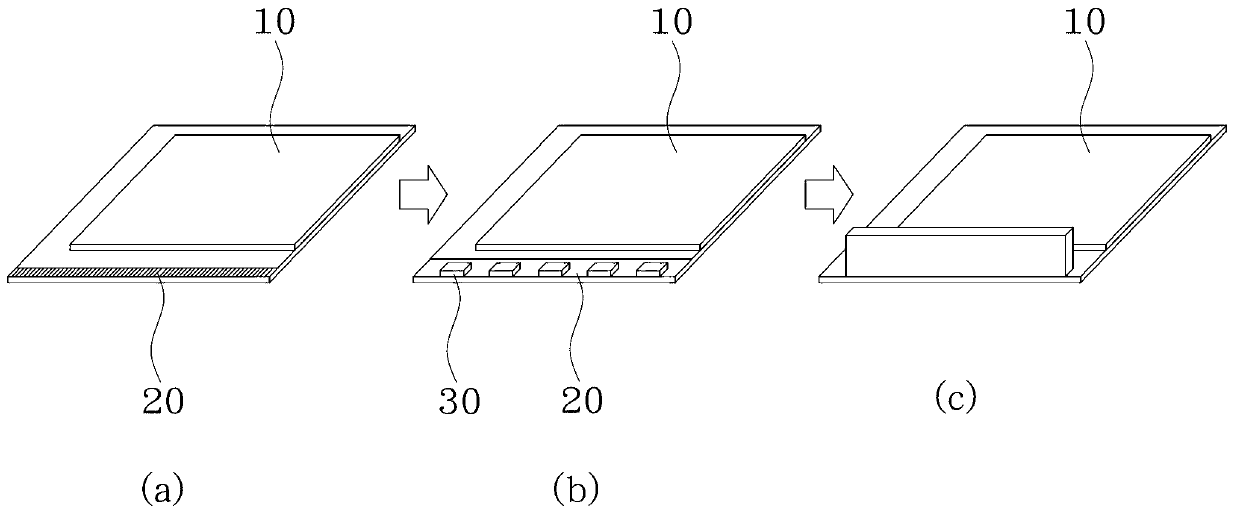
[0026] figure 1 (a) to figure 1 (c) is a schematic diagram showing the process of laminating the driving chip by using the COG process in the liquid crystal display panel in the prior art.

[0027] The liquid crystal display panel includes a glass substrate 10 , and an IC bonding area is disposed on one side of the glass substrate 10 . refer to figure 1 (a), first coat an anisotropic conductive film (ACF) on the corresponding...


PUM


Abstract

The invention provides a liquid crystal display panel, which comprises a printed circuit board component, a glass substrate and an adhesive tape, wherein a jointing area is arranged on one side of the glass substrate; the printed circuit board component and the glass substrate are adhered by means of the adhesive tape; the glass substrate comprises a first surface and a second surface opposite to each other; the jointing area is positioned on the first surface; and the adhesive tape is positioned on the second surface. The adhesive tape is composed of a plurality of discontinuous adhesive strips so that the deformation quantity of the glass substrate is uniformed. Through the application of the liquid crystal display panel, the printed circuit board component and the glass substrate are firmly adhered by means of the adhesive tape, and the adhesive tape is configured to be in a discontinuous manner (such as sectional type or roulette manner), so that the internal pulling stress caused when the glass substrate is in press fit can be inhibited, and COG (Chip On Glass) mura of the panel is improved. Moreover, the deformation space caused by expansion with heat and contraction with cold of the glass substrate can be reserved through the adhesive tape in the discontinuous manner so that the deformation influence due to difference of chip thermal expansion coefficients of the glass substrate and the jointing area is eliminated.

Description

technical field [0001] The invention relates to liquid crystal display technology, in particular to a liquid crystal display panel. Background technique [0002] In recent years, due to the rapid development of electronics and information industry, its related products have become increasingly sophisticated. As far as the current personal computer field is concerned, in addition to seeking higher-speed, more powerful computing units and a variety of peripheral devices to meet user needs, light, thin and small portable mobile devices have gradually become the focus of industry development. field. Taking liquid crystal display as an example, it has the advantages of high image quality, small size, light weight, low voltage drive, low power consumption and wide application range, so it is widely used in portable TVs, mobile phones, projectors, notebook computers , Desktop monitors and other consumer electronics products have become the mainstream of monitors. [0003] As peo...

Claims


Application Information

Patent Timeline
Patent Type & Authority Applications(China)
IPC IPC(8): G02F1/13
Inventor 吴国华林世雄杨慎东高诚壕
Owner AU OPTRONICS (SUZHOU) CORP LTD
Why Eureka
Try Eureka