Method for increasing board utilization rate during manufacture of PCB (printed circuit board)
A PCB board and utilization rate technology, which is applied in the field of PCB manufacturing, can solve the problem of high cost of board materials, and achieve the effect of cost saving
- Summary
- Abstract
- Description
- Claims
- Application Information
AI Technical Summary
Problems solved by technology
Method used
Image
Examples
Embodiment 1
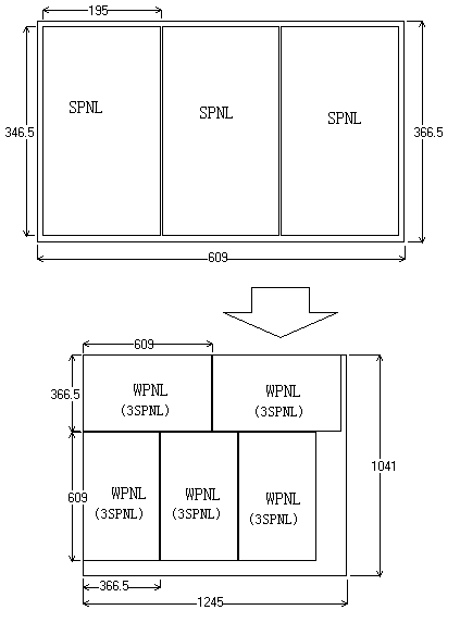
[0016] Such as figure 1 As shown, taking a 2-layer board as an example, if the size of the SPNL board provided by the customer is: 346.5*195mm, the board edge design according to the industry custom is generally to add 10mm to each side of the X and Y directions, and three unit boards are one Board group, the gap between each unit board is set to 2mm, then each board group: X=346.5+20=366.5mm, Y=195*3+4+20=609mm, if the selected board size is: 41* 49 (1041*1245mm), utilization rate: 78%.
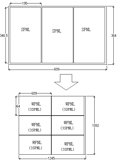
[0017] If it is changed to an asymmetrical edge, such as figure 2 As shown, the side of the board in the X direction is designed to be large (increased by 10mm) and small (increased by 7.5mm), the utilization rate will be much higher, and the substrate will be well utilized, as follows:
[0018] X=346.5+(10+7.5)=364mm, 195*3+4+20=609mm, the selected substrate is: 43*49 (1092*1245mm), the utilization rate is increased to 89.5%, and the remaining waste of the board is very little.
PUM
 Abstract
Description
Claims
Application Information

