Electrostatic discharge protection device

An electrostatic discharge protection and electrode technology, which is applied in the field of electrostatic discharge protection devices, can solve problems such as the inability to effectively control the maintenance voltage and the failure of integrated circuits, and achieve the effect of preventing noise from being triggered by mistake and increasing the trigger voltage

Active Publication Date: 2013-04-10
CSMC TECH FAB2 CO LTD
View PDF5 Cites 3 Cited by
  • Summary
  • Abstract
  • Description
  • Claims
  • Application Information

AI Technical Summary

Problems solved by technology

The disadvantage of this structure is that the maintenance voltage cannot be effectively controlled, and the risk of failure of the integrated circuit due to the latch-up effect cannot be solved.

Method used


Image

  • Electrostatic discharge protection device
  • Electrostatic discharge protection device
  • Electrostatic discharge protection device

Examples


Embodiment Construction

[0014] The following introduces some of the possible embodiments of the present invention, which are intended to provide a basic understanding of the present invention, but are not intended to identify key or decisive elements of the present invention or limit the scope of protection. In the drawings, for the sake of clarity, the thickness of layers or the area of ​​regions may be exaggerated, but as a schematic diagram, it should not be regarded as strictly reflecting the proportional relationship of geometric dimensions. In the drawings, the same reference numerals refer to the same structural parts, and thus their descriptions will be omitted.

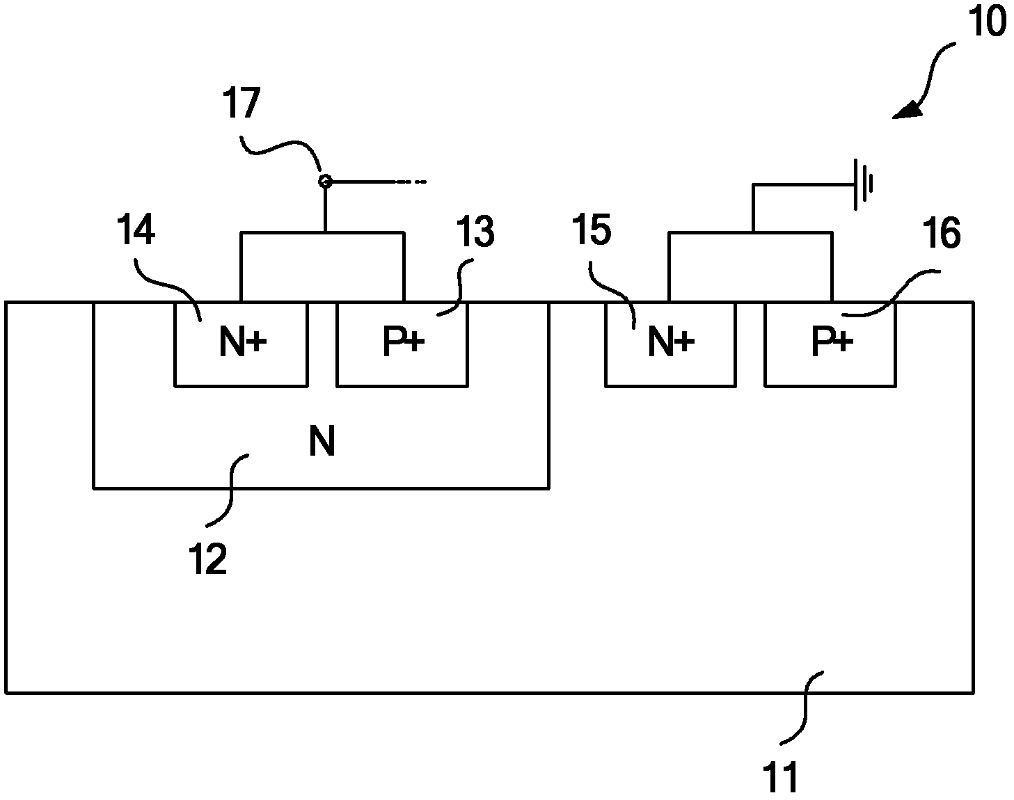
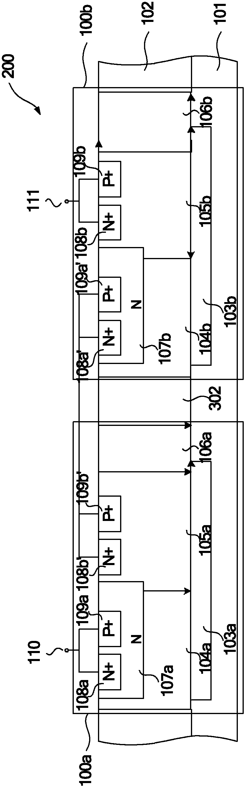
[0015] The present invention provides an electrostatic discharge protection device. In a feasible implementation manner, the electrostatic discharge protection device is based on the epitaxial wafer high-voltage process. image 3 It is a schematic cross-sectional view of a specific embodiment of the electrostatic discharge protectio...


PUM


Abstract

The invention provides an electrostatic discharge protection device. An electrostatic discharge (ESD) mixture filling layer is led to a positive-negative-positive-negative (PNPN) structure, proper trigger voltage is decided through adjustment for filling energy and dosage of the ESD mixture injection layer, proper maintenance voltage is obtained through adjustment for the size of the ESD mixture filling layer, and the latch-up problem is prevented. According to the electrostatic discharge protection device, self-insulation effects are formed based on an extension wafer high voltage process or a silicon-on-insulator (SOI) wafer high voltage process, a component can be prevented from being triggered by noise, and the trigger voltage can be conveniently increased through single electrostatic discharge protection units in serial connection.

Description

technical field [0001] The invention relates to a semiconductor structure, in particular to an electrostatic discharge protection device. Background technique [0002] Electrostatic Discharge (ESD) is a common natural phenomenon in our lives, but the large current generated in a short period of time during electrostatic discharge will cause fatal damage to integrated circuits, which is the cause of failure in the production and application of integrated circuits important question. For example, for the electrostatic discharge phenomenon (Human-BodyModel, HBM) that occurs on the human body, it usually occurs within hundreds of nanoseconds, and the maximum current peak value may reach several amperes. Some other modes, such as machine model (Machine Model, MM) and component charging model (Charged-Device Model, CDM), the electrostatic discharge occurs for a shorter time and the current is larger. Such a large current passes through the integrated circuit in a short period of...

Claims


Application Information

Patent Timeline
Patent Type & Authority Applications(China)
IPC IPC(8): H01L27/02H02H9/04
Inventor 代萌
Owner CSMC TECH FAB2 CO LTD
Why Eureka
Try Eureka