Communication electronic device and antenna structure thereof

An electronic device and antenna structure technology, applied in the field of communication systems, can solve the problems of wasting internal space of the device and affecting antenna characteristics, etc.

Inactive Publication Date: 2013-04-10
ACER INC
View PDF15 Cites 3 Cited by
  • Summary
  • Abstract
  • Description
  • Claims
  • Application Information

AI Technical Summary

Problems solved by technology

For example, in the prior art, such as US Patent No. 7768466B2 "Multiband folded loop antenna (Multiband folded loop antenna)" discloses a communication electronic device with a multiband loop antenna, the loop antenna It is arranged on one edge of the ground element and occupies the entire edge to achieve broadband operation. However, this antenna

Method used


Image

  • Communication electronic device and antenna structure thereof
  • Communication electronic device and antenna structure thereof
  • Communication electronic device and antenna structure thereof

Examples


Embodiment Construction

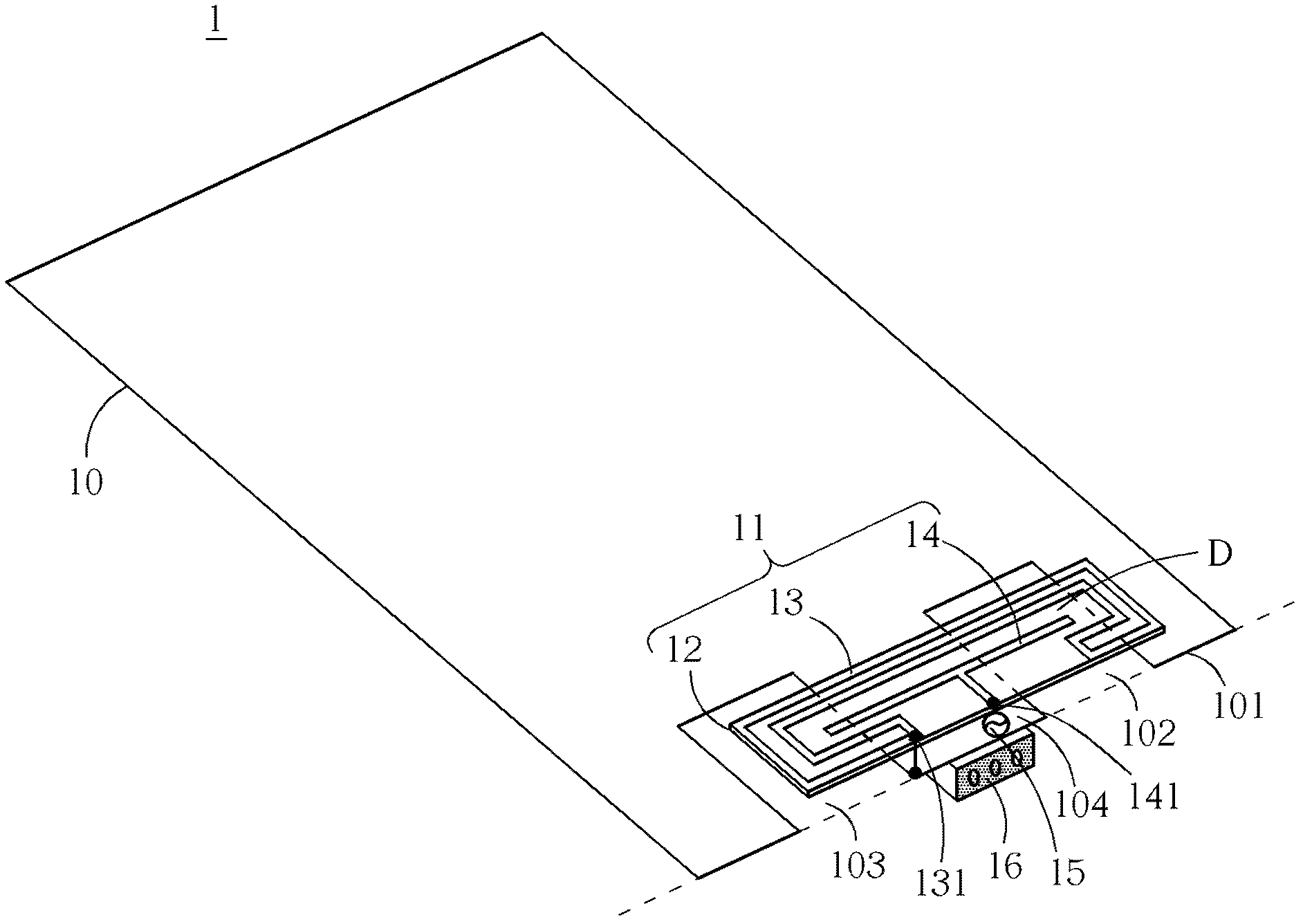
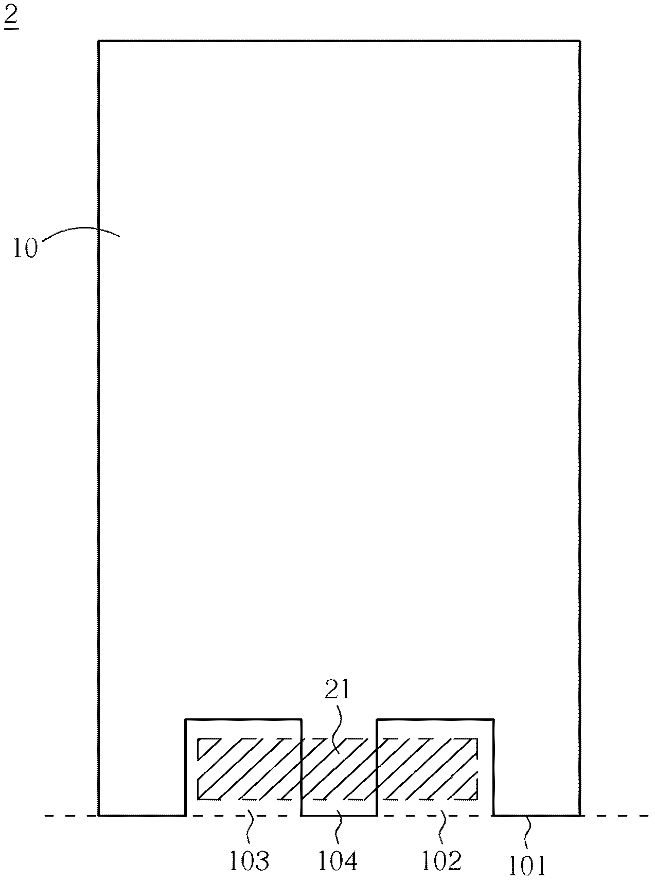
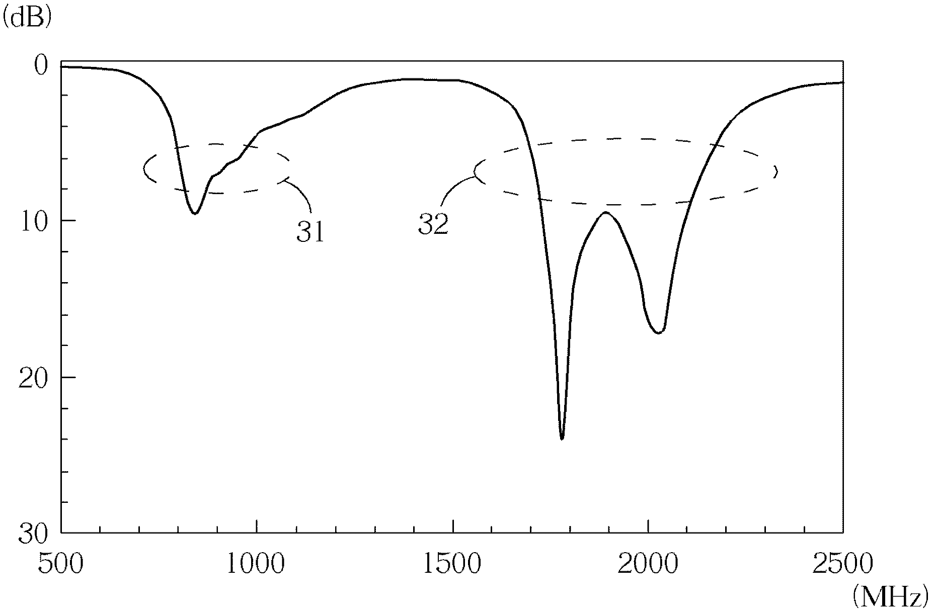
[0032] In order to make the above and other objects, features and advantages of the present invention more comprehensible, specific embodiments of the present invention are listed below and described in detail in conjunction with the accompanying drawings.

[0033] Certain terms are used in the specification and preceding claims to refer to particular elements. Those skilled in the art should understand that hardware manufacturers may use different terms to refer to the same element. The description and the previous claims do not use the difference in name as the way to distinguish components, but use the difference in function of the components as the criterion for distinguishing. The term "comprising" mentioned throughout the specification and the previous claims is an open-ended term, so it should be interpreted as "including but not limited to". In addition, the term "coupled" herein includes any direct and indirect means of electrical connection. Therefore, if it is des...


PUM


Abstract

The invention discloses a communication electronic device which comprises a grounding element and an antenna element. One edge of the grounding element is provided with a first gap, a second gap and a first protrusion portion, neither the first gap nor the second gap is located in the corner of the edge, the first protrusion portion is arranged between the first gap and the second gap; the antenna element and the grounding element are located in different planes, the antenna element has a projection on the grounding element, and the projection is covered on part sections of the first protrusion portion, the first gap and the second gap.

Description

technical field [0001] The present invention relates to a communication system, more specifically, to a communication electronic device and its antenna structure. Background technique [0002] In recent years, due to the advancement of mobile communication technology, communication electronic devices have become a part of many people's lives, and the living environment is also full of electromagnetic waves of different operating systems. Therefore, the impact of electromagnetic waves on users has become a subject that has attracted much attention, especially Communication electronic devices that are in contact with users for a long time, such as mobile phones, tablet computers, etc. But on the other hand, the influence of the hand of the user on the characteristics of the built-in antenna of the communication electronic device has also become an important issue. For example, in the prior art, such as US Patent No. 7768466B2 "Multiband folded loop antenna (Multiband folded l...

Claims


Application Information

Patent Timeline
IPC IPC(8): H04B1/38H04M1/02H01Q1/36H01Q7/00H01Q5/00H01Q1/22
Inventor 翁金辂高也钧
Owner ACER INC
Why Eureka
Try Eureka