Image display device

An image display device and capacitor technology, applied in static indicators, nonlinear optics, instruments, etc., can solve the problems of different stable states, decreased display quality, uneven display, etc., and achieve the effect of eliminating afterimages

Active Publication Date: 2013-04-24
JOLED INC
View PDF9 Cites 6 Cited by
  • Summary
  • Abstract
  • Description
  • Claims
  • Application Information

AI Technical Summary

Problems solved by technology

That is, in the case where the display pattern is different in the previous display period and the subsequent display period, the voltage applied to the gate voltage of the driving TFT is different, thus causing the electrical characteristics of the driving TFT to be different due to the application of the gate voltage in the previous display period. and the stable state of the electrical characteristics of the driving TFT during the subsequent display period when a gate voltage different from that of the previous display period is applied.
Therefore, there is a problem that display unevenness (blotch, afterimage) caused by the influence of the previous display period is displayed at the moment of switching from the previous display period to the next display period, and the display quality is degraded.

Method used


Image

  • Image display device
  • Image display device
  • Image display device

Examples


Embodiment approach 1

[0116] Hereinafter, embodiments of the present invention will be described with reference to the drawings.

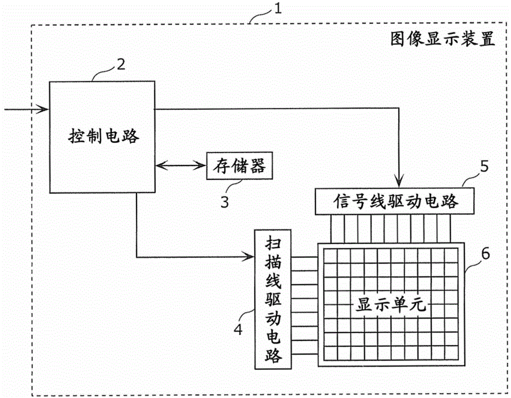
[0117] figure 1 It is a block diagram showing the electrical configuration of the image display device of the present invention. figure 1 The image display device 1 in FIG. 1 includes a control circuit 2 , a memory 3 , a scanning line driving circuit 4 , a signal line driving circuit 5 , and a display unit 6 .

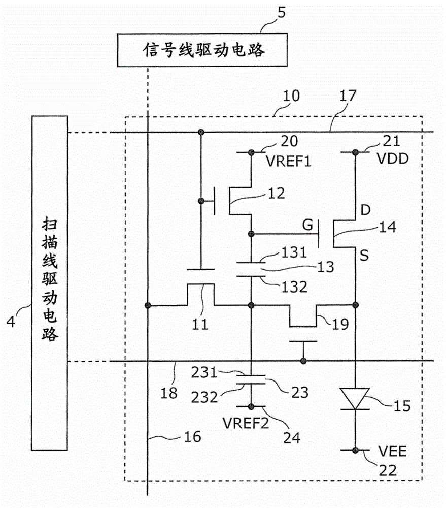
[0118] in addition, figure 2 It is a diagram showing a circuit configuration of a light-emitting pixel included in the display unit according to Embodiment 1 of the present invention and connections to peripheral circuits thereof. figure 2 The light-emitting pixel 10 in the LED includes switching transistors 11, 12 and 19, electrostatic holding capacitors 13 and 23, driving transistor 14, organic EL element 15, signal line 16, scanning lines 17 and 18, reference power supply lines 20 and 24, positive power supply lines 21. Negative power line 22. In addi...

Embodiment approach 2

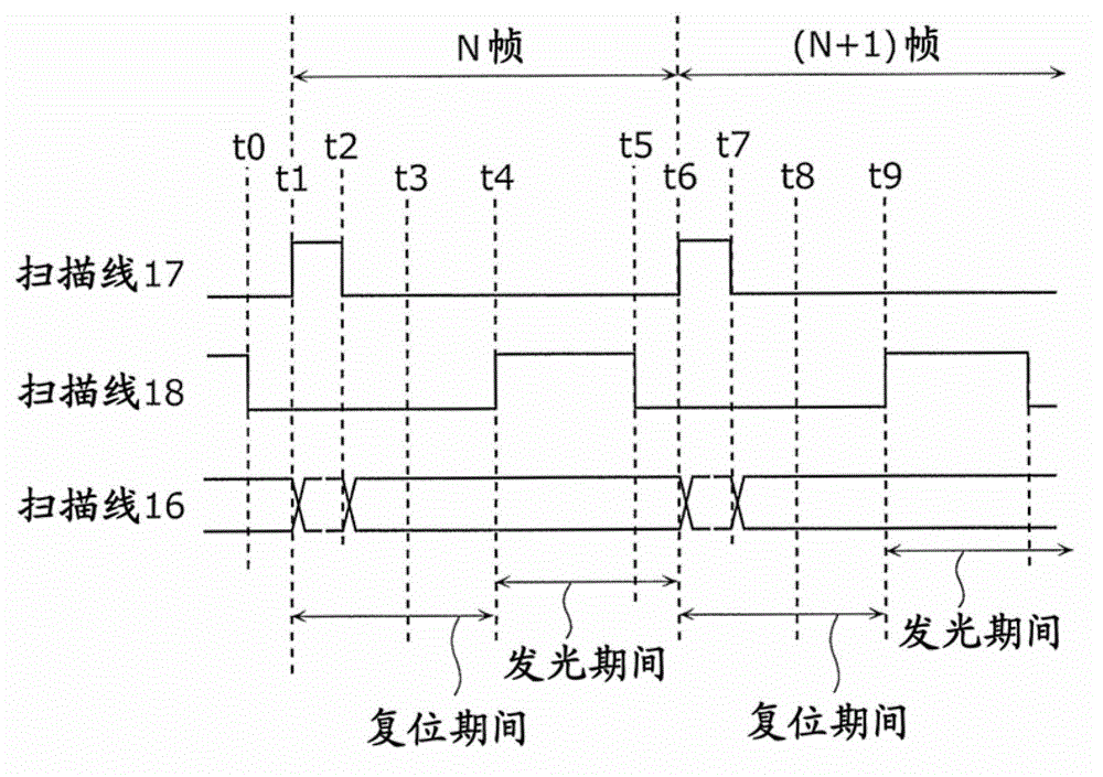
[0184] In Embodiment 1, an example of the control method in the case where the signal propagation delay when the scanning line drive circuit 4 applies the on-voltage to the scanning line 17 is not taken into account has been described. On the other hand, in Embodiment 2, an example of a control method in consideration of a signal transmission delay of the scanning line 17 will be described.

[0185] First, use figure 1 and figure 2 The signal transmission delay of the scanning line 17 will be described.

[0186] The signal transmission delay of the scan line 17 is caused by the wiring resistance of the scan line 17 itself and other control lines and power lines such as the signal line 16, the scan line 18, the reference power line 20, the positive power line 21 or the negative power line 22, etc. The resulting capacitance is specified. That is, when the output of the scanning line driving circuit 4 applied to the scanning line 17 is switched from the on voltage to the off...

Embodiment approach 3

[0201] In Embodiment 1 and Embodiment 2, an example of the control method of the image display device was described. In Embodiment 3, on the basis of Embodiments 1 and 2, afterimages caused by hysteresis characteristics of drive transistors are eliminated by appropriately performing wiring layout of the image display device, which will be described below.

[0202] Hereinafter, problems in the case where the wiring layout is not properly performed will first be described, and then the wiring layout of the image display device in this embodiment will be described.

[0203] For example, it is an important function for the switching transistor 12 to stably hold the gate voltage ( VREF1 ) of the driving transistor 14 together with the electrostatic holding capacitor 13 without leaking during the reset period. Here, the reset period is after the voltage level of the scanning line 17 changes from a high level (on voltage) to a low level (off voltage) as described above (for example, ...


PUM


Abstract

This image display device, which, in a simple pixel circuit, is capable of eliminating afterimages due to the hysterisis characteristics of a drive transistor (14), is provided with: an organic electroluminescent element (15); an electrostatic capacitor (13); a drive transistor (14) having a gate connected to an electrode (131) of the electrostatic capacitor (13), and a source connected to the anode of the organic electroluminescent element (15); an electrostatic capacitor (23) having an electrode (231) connected to an electrode (132) of the electrostatic capacitor (13); a negative power wire (22) for determining the potential of the cathode of the organic electroluminescent element (15); and a scanning line drive circuit (4) for controlling a switching transistor 12, a switching transistor 11 and a switching transistor 19. In the scanning line drive circuit (4), in a non-light-emitting period, a fixed voltage corresponding to the potential of the negative power wire (22) is set to a source electrode of the drive transistor (14) during a period from when a reset period starts to when the non-light-emitting period ends.

Description

technical field [0001] The present invention relates to an image display device, and more particularly, to an image display device using a current-driven light-emitting element. Background technique [0002] As an image display device using a current-driven light-emitting element, an image display device using an organic electroluminescence (EL) element is known. An organic EL display device using such a self-luminous organic EL element does not require a backlight required for a liquid crystal display device, and thus is most suitable for thinning the device. In addition, since the viewing angle is also not limited, its practical use as a next-generation display device is expected. In addition, in the organic EL element used in the organic EL display device, the luminance (brightness) of each light-emitting element is controlled by the current value flowing therein, and the luminance of the liquid crystal cell is controlled by the voltage applied thereto. are different. ...

Claims


Application Information

Patent Timeline
IPC IPC(8): G09G3/30G09G3/20
CPCG09G3/3266G02F1/00G09G3/3233G09G2300/0819G09G2300/0852G09G2320/045G09G3/30
Inventor 小野晋也戎野浩平
Owner JOLED INC
Why Eureka
Try Eureka