
Eureka
For R&D, Eureka makes reading and utilizing patents & technical documents easy.
Eureka AIR
Designed for self-driven R&D workflows. Generate viable solutions, solve complex R&D challenges, empower your innovation with AI.

Eureka Materials
Designed for material experts only. Revolutionize your material R&D, from search, analyze, to developing new materials.

TechResearch
Generate reliable direction feasibility study reports for your R&D in just a few steps.

TechSeek
Discover and master advanced knowledge NOW. Basics, ideas, possibilities, all at once.

TechMind
As an expert in R&D Theories, TechMind can generates customized viable solutions instantly.

TechRisk
Analyze your overall solution with one click, know your potential R&D risks in advance.

TechMonitor
Get weekly tech updates, stay abreast of the latest tech innovations and key insights.
Array substrate of flat panel display device and manufacturing method thereof
An array substrate and flat-panel display technology, used in semiconductor/solid-state device manufacturing, optics, instruments, etc., can solve the problems of increasing signal delay and increasing resistance, and achieve the effect of preventing signal delay, reducing failure rate, and improving process yield
- Summary
- Abstract
- Description
- Claims
- Application Information
AI Technical Summary
Problems solved by technology
Method used
Image

Examples
Embodiment Construction
[0049] Hereinafter, an array substrate of a flat display device and a manufacturing method thereof according to preferred embodiments of the present invention will be described in detail with reference to the accompanying drawings.
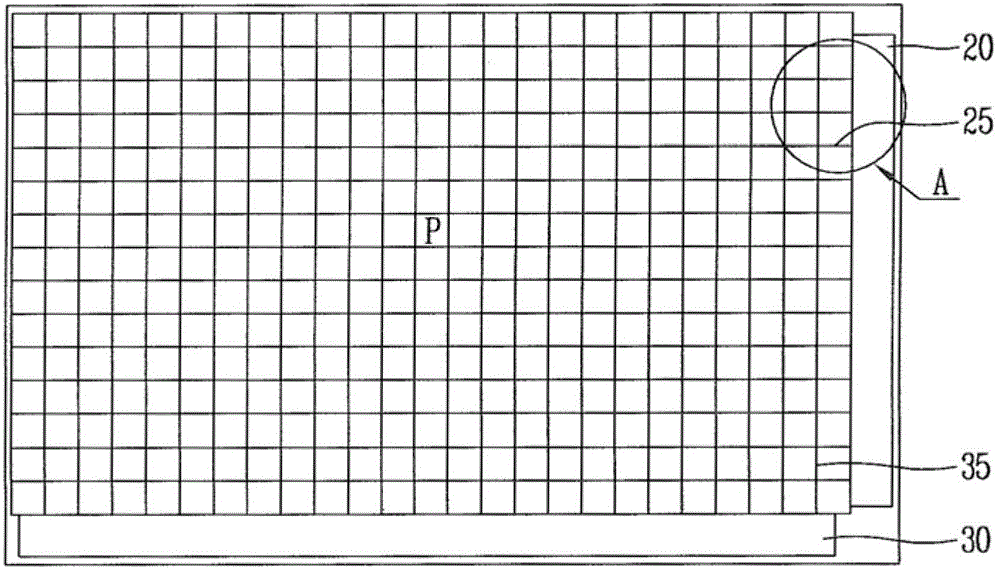
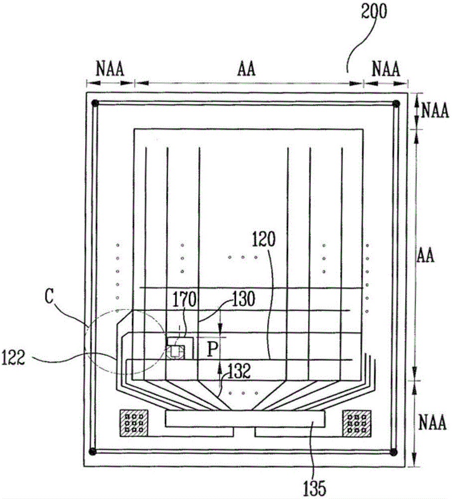
[0050] image 3 is a plan view showing a flat display device according to an embodiment of the present invention.
[0051] refer to image 3 , the array substrate 200 of the flat display device according to the present invention may include a display area (AA) for realizing an image and a non-display area (NAA) disposed at an edge of the display area (AA).
[0052] The array substrate 200 of the flat display device may be formed with a plurality of gate lines 130 for receiving gate signals on a base substrate such as glass or the like, and a plurality of data lines 130 vertically intersecting the plurality of gate lines 130. Line 120. A plurality of pixel regions (P) are defined at intersections of the gate lines and the data lines. A thin fil...
PUM
 Abstract
Description
Claims
Application Information
 - R&D Engineer
- R&D Manager
- IP Professional
- Industry Leading Data Capabilities
- Powerful AI technology
- Patent DNA Extraction
Browse by: Latest US Patents, China's latest patents, Technical Efficacy Thesaurus, Application Domain, Technology Topic, Popular Technical Reports.
© 2024 PatSnap. All rights reserved.Legal|Privacy policy|Modern Slavery Act Transparency Statement|Sitemap|About US| Contact US: help@patsnap.com