Manufacturing method of high-order multistage HDI (High Density Interconnection) printed circuit board

A printed circuit board and manufacturing method technology, applied in the direction of multi-layer circuit manufacturing, etc., can solve the problems of blind hole stacking hole dislocation, blind/through hole and circuit pattern expansion and shrinkage inconsistent, pattern shift and other problems

Active Publication Date: 2013-06-26
MEIZHOU ZHIHAO ELECTRONICS TECH
View PDF7 Cites 46 Cited by
  • Summary
  • Abstract
  • Description
  • Claims
  • Application Information

AI Technical Summary

Problems solved by technology

[0004] The technical problem mainly solved by the present invention is that the existing high-level multi-level HDI printed circuit board manufacturing method causes

Method used


Image

  • Manufacturing method of high-order multistage HDI (High Density Interconnection) printed circuit board
  • Manufacturing method of high-order multistage HDI (High Density Interconnection) printed circuit board
  • Manufacturing method of high-order multistage HDI (High Density Interconnection) printed circuit board

Examples


Embodiment Construction

[0026] The following will clearly and completely describe the technical solutions in the embodiments of the present invention. Obviously, the described embodiments are only some of the embodiments of the present invention, rather than all the embodiments. Based on the embodiments of the present invention, all other embodiments obtained by persons of ordinary skill in the art without making creative efforts belong to the protection scope of the present invention.

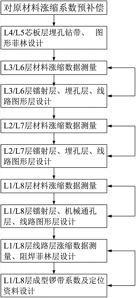
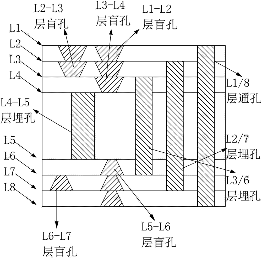
[0027] The invention discloses a method for making a high multi-level HDI printed circuit board, please refer to Figure 1 to Figure 4 , the production method of the present invention is illustrated below with 8 layers of 3-order HDI products, and the production method comprises the following steps:

[0028] Step S1, carry out drilling pre-compensation for the mechanical buried holes of the L4 / L5 layer core board: according to the laminated structure, the characteristics of the core board material, and the expansion ...


PUM


Abstract

The invention discloses a manufacturing method of a high-order multistage HDI (High Density Interconnection) printed circuit board. An expansion coefficient of a cross-band veneer is pre-compensated according to a layer number, a dead hole stacking number and an engineering pre-designed lamination structure of a product, a press frequency and a material characteristic; a reference target coordinate, a shape, a size, a process aligning manner and the like are aligned for design demands for systematizing different graph levels and production positioning reference points, so that the alignment matching index and the expansion alignment precision among different levels and different components can be achieved; all the alignment problems caused by various factors in a production process of a three-stage HDI printing circuit can be considered; the alignment problems among a series of important PCB (Printed Circuit Board) processes, such as an inner layer graph, a secondary outer layer circuit, a secondary outer layer buried hole, an outer layer circuit, a mechanical through hole, a radiation dead hole and solder resistance of a one-stage HDI product, a two-stage HDI product and a three-stage HDI product, can be solved; and meanwhile, the hole overlapping precision of micro dead holes and the alignment precision matching indexes of the dead holes, the through hole and a circuit graph can be ensured.

Description

technical field [0001] The invention relates to the field of printed circuit board (PCB) engineering design and production process, in particular to a method for manufacturing a high-level multi-level HDI printed circuit board. Background technique [0002] With the current trend of continuous and rapid miniaturization, portability and multi-functionalization of electronic products, and the development of high-density mounting technology, the industry has increasingly put forward higher requirements for the carrier and connector printed circuit board as the original component. , so that it can become an electronic component with high density, high precision, and high reliability that can greatly increase the assembly density. Therefore, the high density interconnection (HDI) applied to the new PCB process technology is widely used in various electronic products, and the application range of HDI board technology is becoming wider and wider. [0003] Since high-level multi-le...

Claims


Application Information

Patent Timeline
IPC IPC(8): H05K3/46
Inventor 刘亚辉戴晖刘喜科
Owner MEIZHOU ZHIHAO ELECTRONICS TECH
Why Eureka
Try Eureka