Optical proximity effect correction method and corresponding mask pattern forming method

A technology of optical proximity effect and mask pattern, which is applied in optics, components for photomechanical processing, photomechanical equipment, etc., and can solve problems such as poor correction accuracy

Active Publication Date: 2013-07-03
WUXI DISI MICROELECTRONICS CO LTD
View PDF5 Cites 2 Cited by
  • Summary
  • Abstract
  • Description
  • Claims
  • Application Information

AI Technical Summary

Problems solved by technology

[0005] One way to avoid the above-mentioned deviation is the optical proximity correction method (OPC). During the simulation process using this method, the designed lithographic pattern is continuously corrected so that the corrected designed lithographic pattern is formed as After the mask pattern, the deviation between the mask pattern and the lithographic pattern formed after the final transfer to the silicon wafer is as small as possible, but the current optical proximity effect correction method is not accurate enough

Method used


Image

  • Optical proximity effect correction method and corresponding mask pattern forming method
  • Optical proximity effect correction method and corresponding mask pattern forming method
  • Optical proximity effect correction method and corresponding mask pattern forming method

Examples


Embodiment Construction

[0018] Further illustrate the present invention below in conjunction with accompanying drawing. Those skilled in the art can understand that the following is only to describe the gist of the present invention in conjunction with specific embodiments, and does not limit the implementation of the present invention. The scope of the present invention is determined by the appended claims, and any modifications and changes that do not deviate from the spirit of the present invention shall be covered by the claims of the present invention.

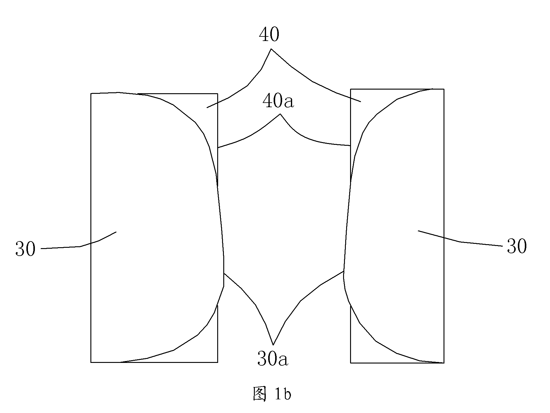
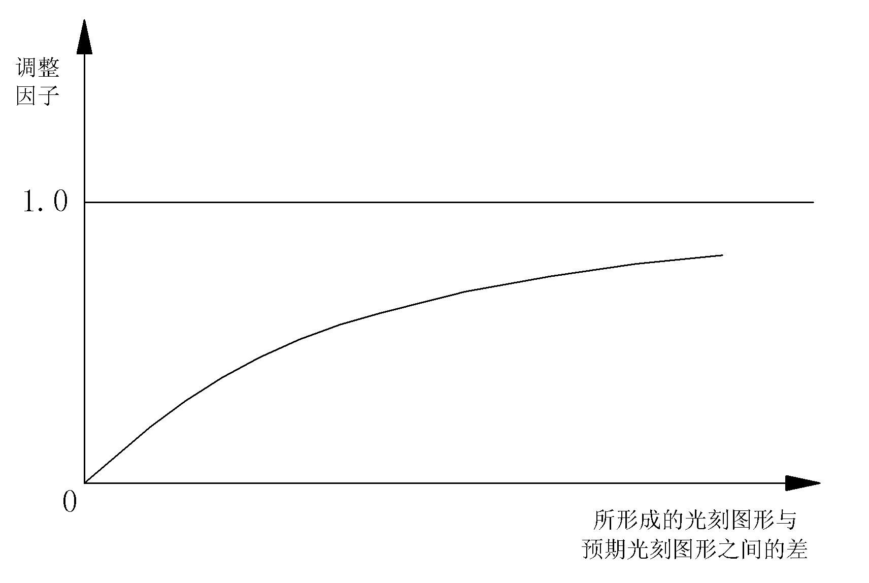
[0019] In the present invention, the term "anticipated lithography pattern" refers to the lithography pattern expected to be obtained on the silicon wafer, which can also be referred to as the design pattern; the term "lithography pattern" is as described in the background technology section, It refers to the pattern obtained by transferring the pattern on the mask plate to each layer of material on the silicon surface by using projection li...


PUM


Abstract

The invention provides an optical proximity effect correction method, comprising: simulating a prospective lithography pattern; obtaining a difference between a lithography pattern formed by simulation and the prospective lithography pattern; and regulating the prospective lithography pattern based on the difference. The regulation comprises: based on a preset relation between a regulation factor and the difference between the lithography pattern formed by simulation and the prospective lithography pattern, obtaining the regulating factor corresponding to the difference between the lithography pattern formed by simulation and the prospective lithography pattern, multiplying the difference by the regulating factor to obtain a regulating amount of the lithography pattern formed by simulation and the prospective lithography pattern, and regulating the prospective lithography pattern based on the regulating amount. Based on the method, deviation generation of the prospective lithography pattern can be avoided after a lithography pattern on a silicon chip surface is formed.

Description

technical field [0001] The invention relates to a manufacturing process of a semiconductor device, in particular to deviation processing between a photolithographic pattern and a mask pattern. Background technique [0002] Photolithography is the main process in the manufacture of integrated circuits. Photolithography is mainly to realize the transfer of the pattern on the mask plate (hereinafter referred to as the mask pattern) to each layer of material on the silicon surface. The projected light propagates to the silicon wafer after passing through the mask pattern, so that a lithography pattern related to the mask pattern is obtained on the silicon wafer. For lithography, the mask pattern is equivalent to an obstacle on the propagation route. According to the principle of light wave diffraction and interference, light waves will diffract when passing through the mask, and the light waves at different positions of the mask will also interfere, so the light intens...

Claims


Application Information

Patent Timeline
IPC IPC(8): G03F1/36
CPCG03F1/36G03F1/70G03F7/70441
Inventor 万金垠王谨恒张雷陈洁
Owner WUXI DISI MICROELECTRONICS CO LTD
Why Eureka
Try Eureka