Method for improving arc discharge defect in mim capacitor fabrication

A technology of arc discharge and capacitors, which is applied in semiconductor/solid-state device manufacturing, circuits, electrical components, etc., can solve problems affecting the yield of semiconductor integrated circuits, etc., and achieve the goal of improving arc discharge defects, avoiding arc discharge defects, and improving yield Effect

Active Publication Date: 2015-10-21
SEMICON MFG INT (SHANGHAI) CORP
View PDF3 Cites 0 Cited by
  • Summary
  • Abstract
  • Description
  • Claims
  • Application Information

AI Technical Summary

Problems solved by technology

It can be seen that the arc discharge defects of MIM capacitors seriously affect the yield of semiconductor integrated circuits

Method used


Image

  • Method for improving arc discharge defect in mim capacitor fabrication
  • Method for improving arc discharge defect in mim capacitor fabrication
  • Method for improving arc discharge defect in mim capacitor fabrication

Examples


Embodiment Construction

[0028] The method for improving the arc discharge defect in the manufacture of MIM capacitors proposed by the present invention will be further described in detail below in conjunction with the accompanying drawings and specific embodiments.

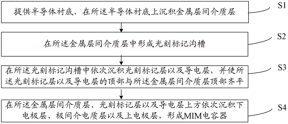
[0029] Such as image 3 As shown, the present invention proposes a kind of method for improving the arc discharge defect in MIM capacitor making, comprising:

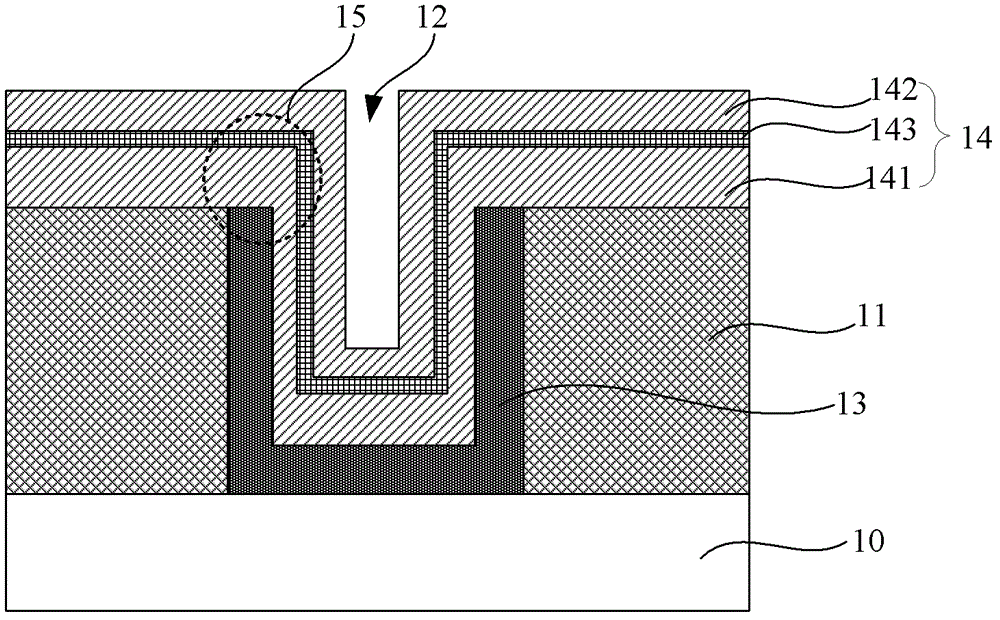
[0030] S1, providing a semiconductor substrate, and depositing an inter-metal dielectric layer on the semiconductor substrate;

[0031] S2, forming a photolithography marking groove in the inter-metal dielectric layer;

[0032] S3, sequentially depositing a photolithographic marking layer and a conductive layer in the photolithographic marking groove, and planarizing to the inter-metal dielectric layer;

[0033] S4, sequentially depositing a lower electrode layer, an interelectrode dielectric layer, and an upper electrode layer on the intermetal dielectric layer and the filled c...


PUM

PropertyMeasurementUnit
widthaaaaaaaaaa

Abstract

The invention provides a method for avoiding an arc discharge defect in a metal-insulator-metal (MIM) capacitor manufacturing process. Before an MIM capacitor is manufactured, a lithography marking trench, used for lithography alignment or measurement, in a metal interlayer dielectric layer is filled at first, and therefore happening conditions of point discharge are eliminated, the arc discharge defect of an upper electrode layer is avoided when the MIM capacitor is manufactured above the metal interlayer dielectric layer and the filled lithography marking trench, and the good product rate of semiconductor integrated circuits is improved.

Description

technical field [0001] The invention relates to the field of semiconductor manufacturing, in particular to a method for improving arc discharge defects in MIM capacitor manufacturing. Background technique [0002] Metal-insulator-metal (metal-insulator-metal, MIM) capacitors have the advantages of low RC value and can maintain a relatively stable operating voltage, and are widely used in very large scale integrated circuits (VLSI, Very Large Scale Integrated circuits) . [0003] With the rapid development of semiconductor technology, the feature size of devices continues to shrink, and high-performance, high-density connections between components are not only interconnected in a single interconnect layer, but also interconnected between multiple layers. Therefore, a large number of connections between devices adopt a multilayer interconnection structure, in which multiple interconnection metal layers are stacked on top of each other, and an interlayer insulating layer is pl...

Claims


Application Information

Patent Timeline
Patent Type & Authority Patents(China)
IPC IPC(8): H01L21/02
Inventor 韩亮张冠群李志超张继伟
Owner SEMICON MFG INT (SHANGHAI) CORP
Why Eureka
Try Eureka