Method for improving arc discharge defects in capacitor fabrication and capacitor

A technology of arc discharge and capacitors, which is applied in the direction of capacitors, electric solid devices, circuits, etc., can solve problems affecting the yield rate of semiconductor integrated circuits, etc., and achieve the effect of improving arc discharge defects, avoiding arc discharge defects, and improving yield

Inactive Publication Date: 2018-12-21
ANHUI POLYTECHNIC UNIV MECHANICAL & ELECTRICAL COLLEGE
View PDF3 Cites 3 Cited by
  • Summary
  • Abstract
  • Description
  • Claims
  • Application Information

AI Technical Summary

Problems solved by technology

It can be seen that the arc discharge defects produced in the traditional process of manufacturing MIM capacitors seriously affect the yield of semiconductor integrated circuits

Method used


Image

  • Method for improving arc discharge defects in capacitor fabrication and capacitor
  • Method for improving arc discharge defects in capacitor fabrication and capacitor
  • Method for improving arc discharge defects in capacitor fabrication and capacitor

Examples


Embodiment Construction

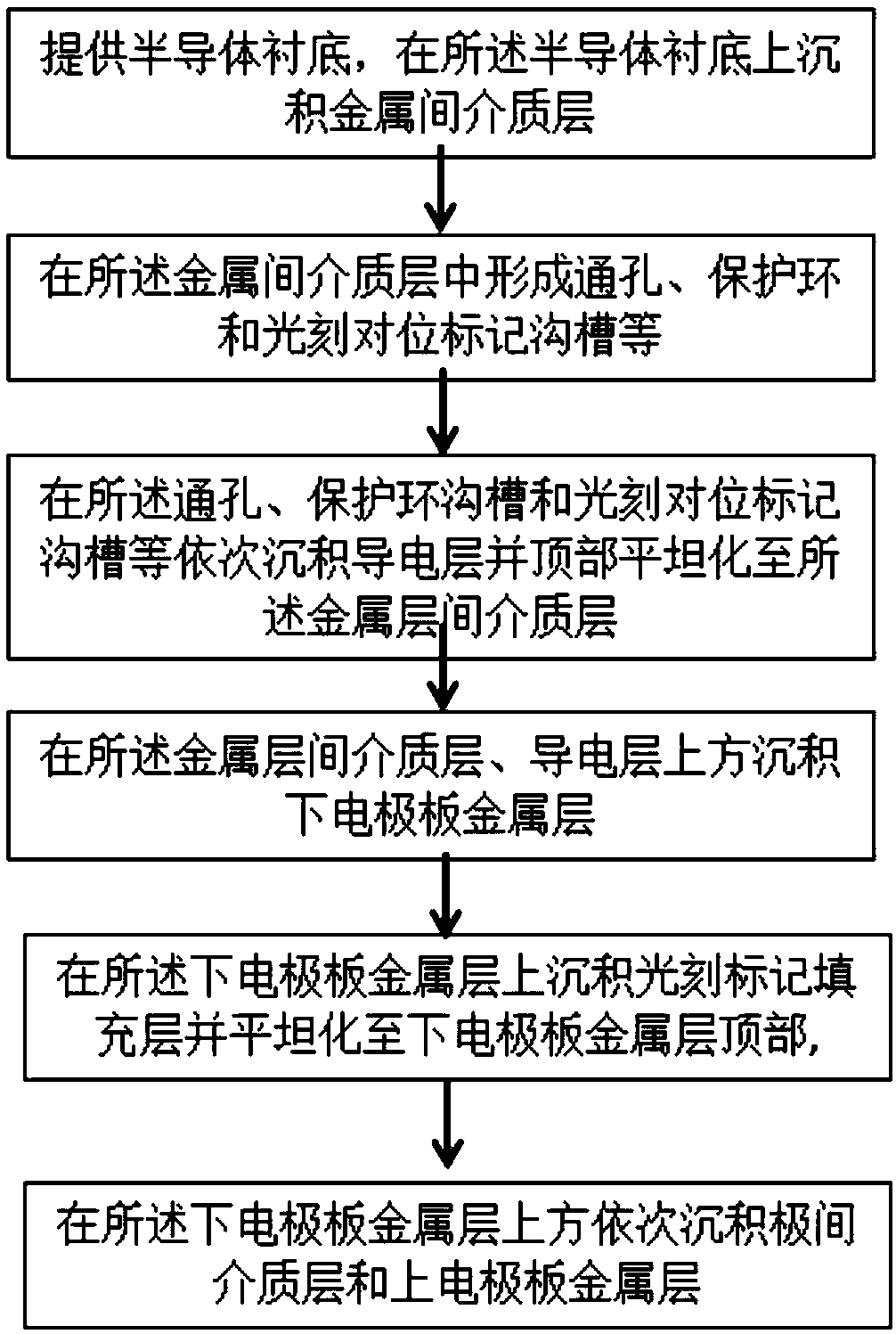
[0030] Specific embodiments of the present invention will be described in detail below in conjunction with the accompanying drawings. It should be understood that the specific embodiments described here are only used to illustrate and explain the present invention, and are not intended to limit the present invention.

[0031] In the present invention, unless stated otherwise, the orientation words included in the term such as "up, down, left, and right" only represent the orientation of the term in the normal use state, or the common name understood by those skilled in the art, rather than should be considered a limitation of the term.

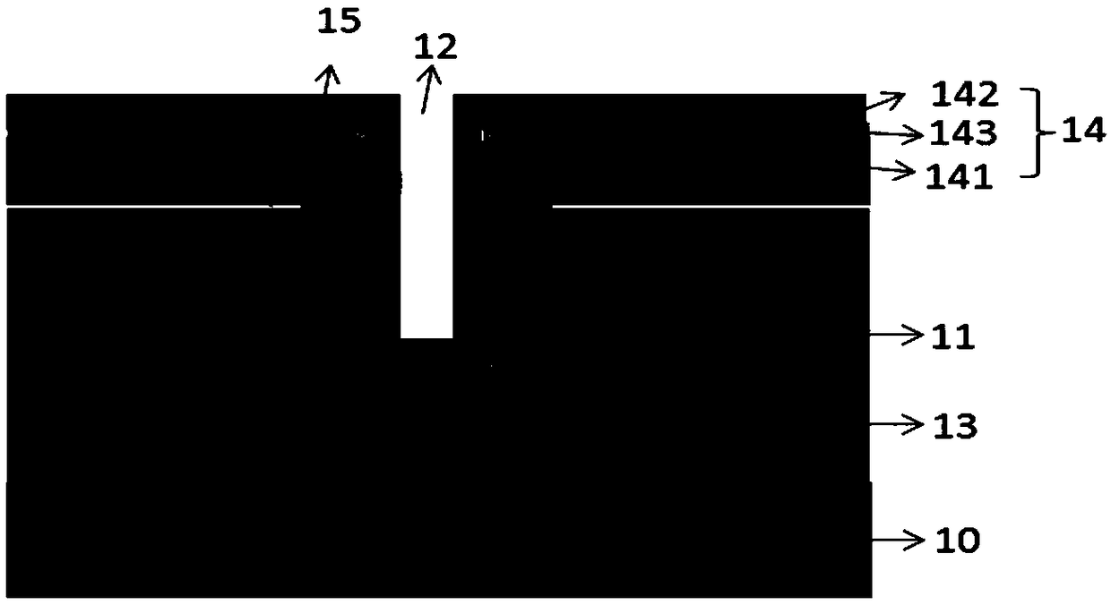
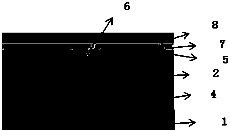
[0032] The invention provides a method for improving arc discharge defects in the manufacture of MIM capacitors. In step 1, an intermetallic dielectric layer 2 is provided on a semiconductor substrate 1, and through holes and photolithographic alignment are provided on the upper surface of the intermetallic dielectric layer 2. Marking the gro...


PUM


Abstract

A method for improving arc discharge defects in MIM capacitor fabrication and a capacitor are disclosed, the method includes such steps of setting an intermetallic dielectric layer on a semiconductorsubstrate, setting a via hole and a photolithography alignment mark trench on the upper surface of the intermetallic dielectric layer, pre-filling a conductive layer (4) on the upper surface of the via hole and the upper surface of photolithography alignment mark; 2, coating the upper surface of the semiconductor substrate (1) and the upper surface of the conductive layer (4) with the metal layerof the lower electrode plate, and forming a photolithographic alignment mark filling layer (6) on the upper surface of the metal layer of the lower electrode plate, wherein the photolithographic alignment mark filling layer (6) can sufficiently fill the photolithographic alignment mark trench; 3, planarizing the photolithographic alignment mark fill layer (6) other than the photolithographic alignment mark trench to the top of the metal lay of the lower electrode plate. The invention overcomes the arc discharge defects generated in the MIM capacitor process in the prior art and avoids the arcdischarge.

Description

technical field [0001] The invention relates to the field of manufacturing electronic components, in particular to a method for improving arc discharge defects in the manufacture of MIM capacitors. Background technique [0002] Since some parts of the above-mentioned MIM capacitors are formed on structures such as a guard ring (seal ring) groove, a photolithography mark groove, and a mark groove in a scribe line, the width of the above-mentioned groove structure is much larger than normal In the process of depositing metal tungsten into the trenches, the trenches cannot be filled, and a structure with sharp corners 15 appears. With the increase of semiconductor integration and the continuous reduction of device feature size, the insulating dielectric layer 143 of the above-mentioned MIM capacitor also becomes very thin, even less than 1000 Å, so it is very important to form the upper electrode layer 142 during PVD deposition of metals such as aluminum. It is easy to generat...

Claims


Application Information

Patent Timeline
IPC IPC(8): H01L23/522
CPCH01L23/5223H01L28/40
Inventor 王晓云杜正宽范宇平
Owner ANHUI POLYTECHNIC UNIV MECHANICAL & ELECTRICAL COLLEGE
Why Eureka
Try Eureka