Capacitors and how to form them
A technology of capacitance and conductive layer, applied in the direction of circuits, electrical components, electric solid devices, etc., can solve the problems of increasing manufacturing costs and achieve the effect of large capacitance and large surface area
- Summary
- Abstract
- Description
- Claims
- Application Information
AI Technical Summary
Problems solved by technology
Method used
Image


Examples
Embodiment Construction
[0057] The inventor obtains a new capacitance forming method through creative work.
[0058] In order to make the above objects, features and advantages of the present invention more comprehensible, specific implementations of the present invention will be described in detail below in conjunction with the accompanying drawings. When describing the embodiments of the present invention in detail, for convenience of explanation, the schematic diagrams will not be partially enlarged according to the general scale, and the schematic diagrams are only examples, which shall not limit the protection scope of the present invention. In addition, the three-dimensional space dimensions of length, width and depth should be included in actual production.
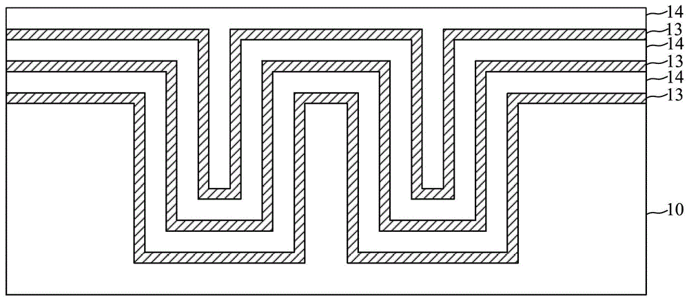
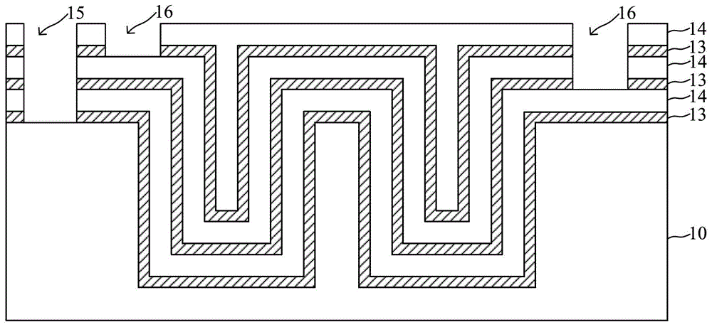
[0059] refer to Image 6 , and combined with the reference Figure 5 , performing step S51 , providing a semiconductor substrate 100 , and forming a first trench 101 in the semiconductor substrate 100 . In a specific embodiment, a plur...
PUM
 Abstract
Description
Claims
Application Information
 - R&D
- Intellectual Property
- Life Sciences
- Materials
- Tech Scout
- Unparalleled Data Quality
- Higher Quality Content
- 60% Fewer Hallucinations
Browse by: Latest US Patents, China's latest patents, Technical Efficacy Thesaurus, Application Domain, Technology Topic, Popular Technical Reports.
© 2025 PatSnap. All rights reserved.Legal|Privacy policy|Modern Slavery Act Transparency Statement|Sitemap|About US| Contact US: help@patsnap.com