multi-chip package

A multi-chip packaging and chip technology, which is applied to electric solid-state devices, semiconductor devices, semiconductor/solid-state device components, etc., can solve the problems of chip and packaging substrate damage, yield decline, cost increase, etc. The effect of transmission delay reduction

Active Publication Date: 2015-12-23
上海鸿隽电子科技有限公司
View PDF5 Cites 0 Cited by
  • Summary
  • Abstract
  • Description
  • Claims
  • Application Information

AI Technical Summary

Problems solved by technology

However, when the thickness is sufficiently thin, further thinning will cause damage to the chip and packaging substrate, seriously affecting the electrical performance of the package, reducing the yield and increasing the cost

Method used


Image

  • multi-chip package
  • multi-chip package
  • multi-chip package

Examples


Embodiment Construction

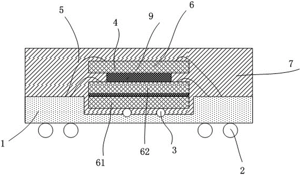
[0027] Generally speaking, semi-open multi-chip packaging technology is commonly seen as figure 1 In the stacked structure shown, a first chip 61 is attached to a groove of a substrate 1 with an upper opening, connected by solder balls 3 or wire bonding, and the second chip 62 is attached to the first chip with the front facing up. On the back side, the second chip 62 is electrically connected to the lead-out end on the upper surface of the substrate 1 by wire bonding, and a blank chip 9 is glued to the middle of the second chip 62, and the third chip 6 is glued on the blank chip 9. The third chip 6 is electrically connected to the corresponding lead-out end on the upper surface of the substrate 1 by wire 5 bonding, and a package body 7 is formed by sealing with resin, and solder balls 2 are planted on the lower surface of the substrate 1 corresponding to the lead-out port of the circuit to form a known A package structure.

[0028] Such as figure 1 The structure shown resul...


PUM


Abstract

The invention discloses a multi-chip package, comprising: a substrate, which is provided with a substrate circuit and has a first surface and a second surface opposite to the first surface, wherein a central groove is formed on the first surface, and a second surface is formed on the second surface. The surface is symmetrically formed with at least one pair of second surface grooves with respect to the center of the central groove; the chip set, each chip is arranged in the central groove and each second surface groove in equal numbers, and is matched with the substrate circuit an electrical connection; and an encapsulation layer, encapsulating the chipset on the substrate, thereby protecting each chip. According to the present invention, the problems of signal transmission delay and signal asynchrony during multi-chip packaging can be effectively reduced.

Description

technical field [0001] The invention relates to a multi-chip package body. Background technique [0002] In the manufacturing process of semiconductor devices, one or more semiconductor chips are mounted on a lead frame or substrate, and the external pins of the chip are connected to the corresponding pins of the substrate by wire bonding or flipchip, sealed with resin, and then sealed with resin. The dicing tool cuts the package substrate to form individual packages with specific functions. [0003] By assembling the above-mentioned individual packages, various semiconductor devices are manufactured, which are widely used in electronic equipment such as micro-electro-mechanical systems, personal computers, mobile phones, and servers. [0004] Since the mid-to-late 1980s, electronic products have been developing toward lightness, thinness, and miniaturization in appearance, and toward networking and multimedia in performance. Requirements on the corresponding appearance ma...

Claims


Application Information

Patent Timeline
Patent Type & Authority Patents(China)
IPC IPC(8): H01L23/485H01L23/488
CPCH01L2924/15311H01L2224/16225H01L2224/73253H01L2224/73265H01L2924/15153H01L2224/16227H01L2224/48227
Inventor 孟新玲刘昭麟隋春飞户俊华栗振超
Owner 上海鸿隽电子科技有限公司
Why Eureka
Try Eureka