A low-voltage high-speed inductive load drive circuit

A technology for driving circuits and inductive loads, applied in electrical digital data processing, instruments, etc., can solve the problems of reduced output amplitude of the driving circuit, out-of-tolerance parameters of high-frequency data zero-crossing interval, large difference in gate-source voltage, etc. The effect of reducing signal transmission delay, preventing oscillation, and meeting communication requirements

Active Publication Date: 2019-07-16
XIAN MICROELECTRONICS TECH INST
View PDF6 Cites 0 Cited by
  • Summary
  • Abstract
  • Description
  • Claims
  • Application Information

AI Technical Summary

Problems solved by technology

If the circuit needs to drive the 4M 1553 bus, since the circuit uses RC charging and discharging, under high-speed conditions, the gate-source voltage of the high-voltage PMOS transistor is about 1V lower than VDD when the MP2 gate capacitance discharges, causing the output amplitude of the drive circuit to decrease; in addition, the 4M When the 1553 bus communicates normally, the data cycle is 125ns, 250ns, 375ns, 500ns. Since the RC charging and discharging circuit is used to control the slope of the driving signal, the gate-source voltage of the high-voltage PMOS transistor MP2 has a large difference when the low-frequency data and high-frequency data are driven. , when low-frequency data transitions to high-frequency data, the zero-crossing interval parameters of high-frequency data are out of tolerance, resulting in the failure of normal communication in the 4M 1553 bus system

Method used


Image

  • A low-voltage high-speed inductive load drive circuit
  • A low-voltage high-speed inductive load drive circuit
  • A low-voltage high-speed inductive load drive circuit

Examples


Embodiment 1

[0044] Based on 0.5um BCD digital-analog mixed-signal process technology, input low level is less than or equal to 0.33V, input high level is greater than or equal to 2.97V, 3.15V≤VDD≤3.45V, can realize normal communication of 32 nodes, at 3.3V power supply voltage Next, the differential amplitude of the near-end node is greater than or equal to 20V, the differential amplitude of the middle-end node is equal to 5V, and the differential amplitude of the remote node is greater than or equal to 0.86V.

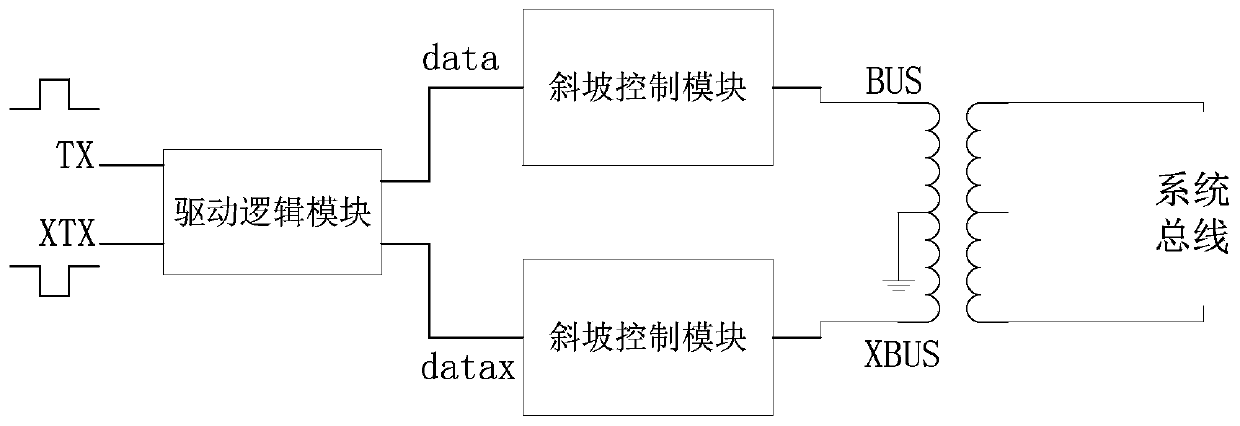
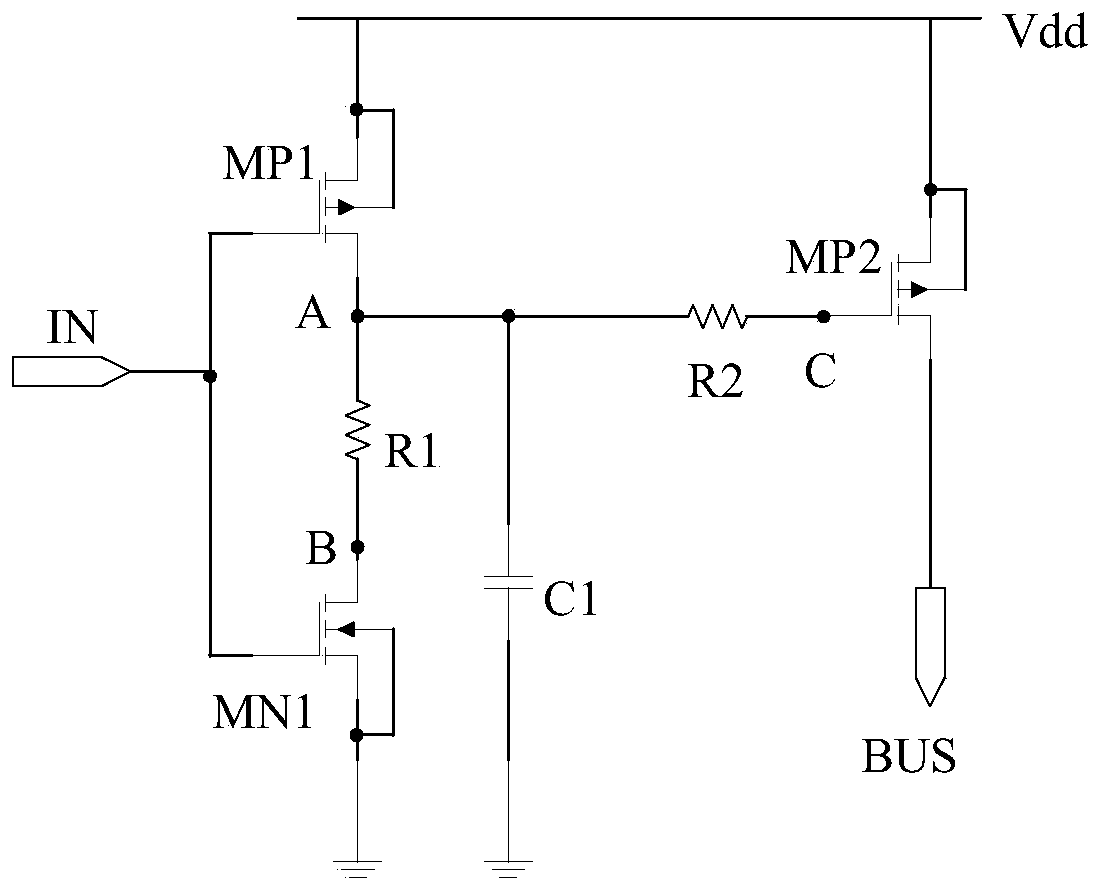
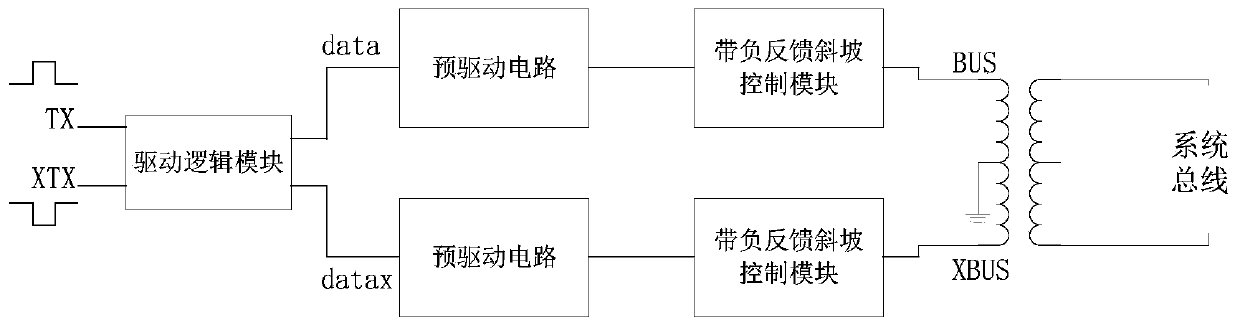
[0045] According to the inventive scheme, under the condition that the electrical connection characteristics of the drive circuit are correct, the communication network can be constructed according to the relevant standards of the 4M 1553 bus. When the 4M 1553 signal drives the bus, when low-frequency data and high-frequency data are transmitted, the gate voltage of the high-voltage PMOS transistor MP4 Both are close to 0V, which ensures that the high-amplitude output of the drive ...


PUM


Abstract

The invention provides a low-voltage high-speed inductive loading driving circuit. High-speed low-voltage high-amplitude outputting can be guaranteed, a zero-passage interval of high-speed data of a bus can also be effectively improved, the communication requirement of a 4M 1553 bus is met, and the communication reliability of a system is improved. The low-voltage high-speed inductive loading driving circuit comprises a driving logic module, pre-driving modules and negative-feedback-slope control modules; a bus signal BUS is output by one pre-driving module and one negative-feedback-slope control module which are sequentially connected with one output end of the driving logic module, and a bus differential signal XBUS is output by another pre-driving module and another negative-feedback-slope control module which are sequentially connected with another output end of the driving logic module; the negative-feedback-slope control modules are used for controlling the positive edge and the negative edge of the bus output signal, and it is prevented that the output signal is subjected to zero returning to be vibrated; the pre-driving modules are used for driving the negative-feedback-slope control modules.

Description

technical field [0001] The invention relates to the technical field of integrated circuits, in particular to a low-voltage high-speed inductive load drive circuit. Background technique [0002] The current structure of the 1M 1553 bus low-voltage drive circuit is as follows: figure 1 As shown, including the drive logic module and the slope control circuit module. The drive logic module is composed of a plurality of NOT gates, NAND gates and NOR gates, which mainly realize signal shaping, differential signal output of TX and XTX, in-phase signal shielding, enable signal control, and realize the logic control of the drive circuit. The ramp control circuit structure is as figure 2 As shown, the charging tube PMOS transistor MP1, the discharging tube NMOS transistor MN1, the RC charging current limiting resistor R2, the RC discharging current limiting resistors R1, R2, the RC time constant capacitor C1 is set, and the bus drives the high voltage PMOS transistor MP2. Among th...

Claims


Application Information

Patent Timeline
Patent Type & Authority Patents(China)
IPC IPC(8): G06F13/40
CPCG06F13/4072
Inventor 季轻舟雒宝花杨力宏李飞强汪西虎
Owner XIAN MICROELECTRONICS TECH INST
Why Eureka
Try Eureka