Line substrate structure and manufacturing method thereof

A technology for circuit substrates and manufacturing methods, applied in the fields of printed circuit manufacturing, improvement of metal adhesion of insulating substrates, printed circuits, etc., can solve problems such as high production costs and consumption, and achieve the effect of reducing catalysts

Inactive Publication Date: 2013-07-24
KUANG HONG PRECISION
View PDF8 Cites 12 Cited by
  • Summary
  • Abstract
  • Description
  • Claims
  • Application Information

AI Technical Summary

Problems solved by technology

[0010] In order to solve the problems existing in the above-mentioned prior art, the object of the present invention is to provide a circuit substrate structure and a manufacturing method thereof, so as to solve the problems of high production cost in the manufacturing process of the existing three-dimensional circuit.

Method used


Image

  • Line substrate structure and manufacturing method thereof
  • Line substrate structure and manufacturing method thereof
  • Line substrate structure and manufacturing method thereof

Examples


Embodiment Construction

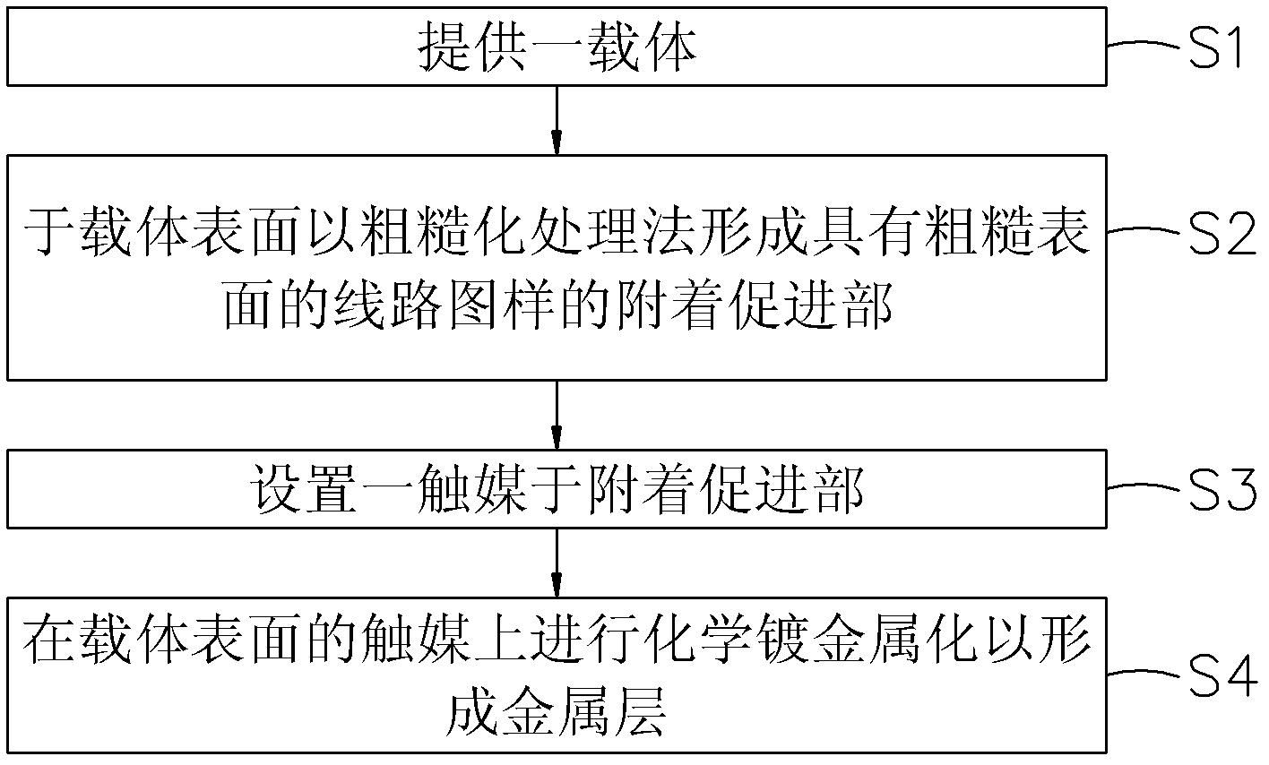
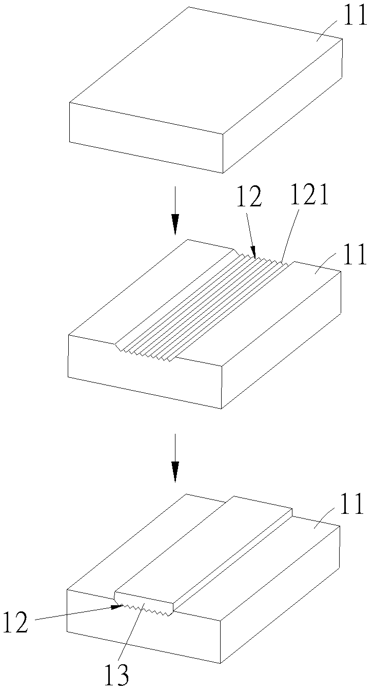
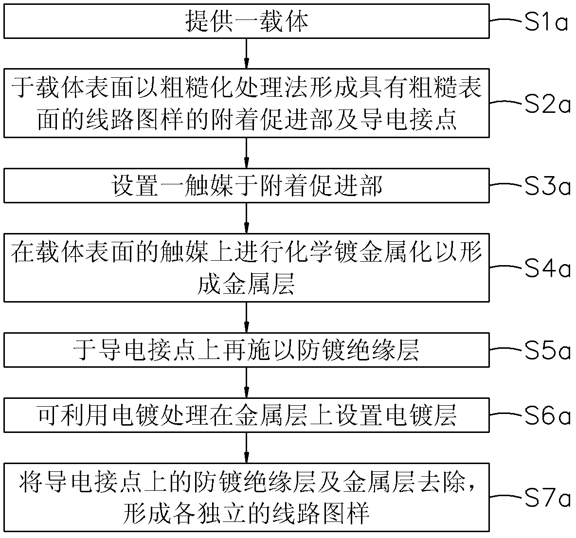
[0052] In order to facilitate the understanding of the technical features, content and advantages of the present invention and the effects that can be achieved, the present invention is now combined with the accompanying drawings, and is described in detail in the form of embodiments as follows, and the accompanying drawings used herein are only intended to For illustrative purposes and to assist the description, it is not necessarily the true proportion and precise configuration of the present invention after implementation. Therefore, the scale and configuration relationship of the attached drawings should not be interpreted to limit the scope of rights of the present invention in actual implementation. In order to understand the technical characteristics and practical effects of the present invention in detail, and to implement them according to the contents of the description, the following examples are now further described in detail as follows.

[0053] The invention prov...


PUM

PropertyMeasurementUnit
wavelengthaaaaaaaaaa

Abstract

The invention discloses a manufacturing method of a line substrate structure and a manufactured product of the substrate structure. The method includes the steps of firstly, forming an attachment promoting portion with a rough surface on the surface of a carrier through a roughness processing method, then, arranging catalytic agents on the surface of the attachment promoting portion, finally, enabling the catalytic agents to react through a chemical planting reduction method, and thus forming a metal layer on the attachment promoting portion. The manufacturing method can effectively reduce the use of the catalytic agents or catalysts and can greatly reduce use cost of the catalytic agents and the catalysts.

Description

technical field [0001] The invention relates to a circuit substrate structure and a manufacturing method thereof, in particular to a method for forming a circuit substrate structure on a non-conductive carrier. Background technique [0002] Based on the current diversification of 3C products, the public pays more attention to the convenience and portability of 3C products, driving electronic products to develop in the direction of miniaturization, light weight and multi-function, and at the same time promoting IC design and its circuit design to three-dimensional The direction of 3D design is developing. Through the three-dimensional design of circuit components, complex circuits can be formed on circuit components with limited volume, so that electronic products can reduce the appearance size and make them more miniaturized and lightweight without affecting their functions. In other words, the three-dimensional design of circuit components enables electronic products to ma...

Claims


Application Information

Patent Timeline
Patent Type & Authority Applications(China)
IPC IPC(8): H05K3/18H05K3/38H05K1/02
Inventor 江振丰江荣泉
Owner KUANG HONG PRECISION
Why Eureka
Try Eureka