Split gate flash memory unit and manufacturing method thereof
A technology for memory cells and separation gates, which is applied in the fields of electrical components, semiconductor/solid-state device manufacturing, electrical solid-state devices, etc. effect, increase the effective thickness, avoid the effect of programming interference
- Summary
- Abstract
- Description
- Claims
- Application Information
AI Technical Summary
Problems solved by technology
Method used
Image

Examples
Embodiment Construction
[0040] In order to make the object, technical solution, and advantages of the present invention clearer, the present invention will be further described in detail below with reference to the accompanying drawings and examples.
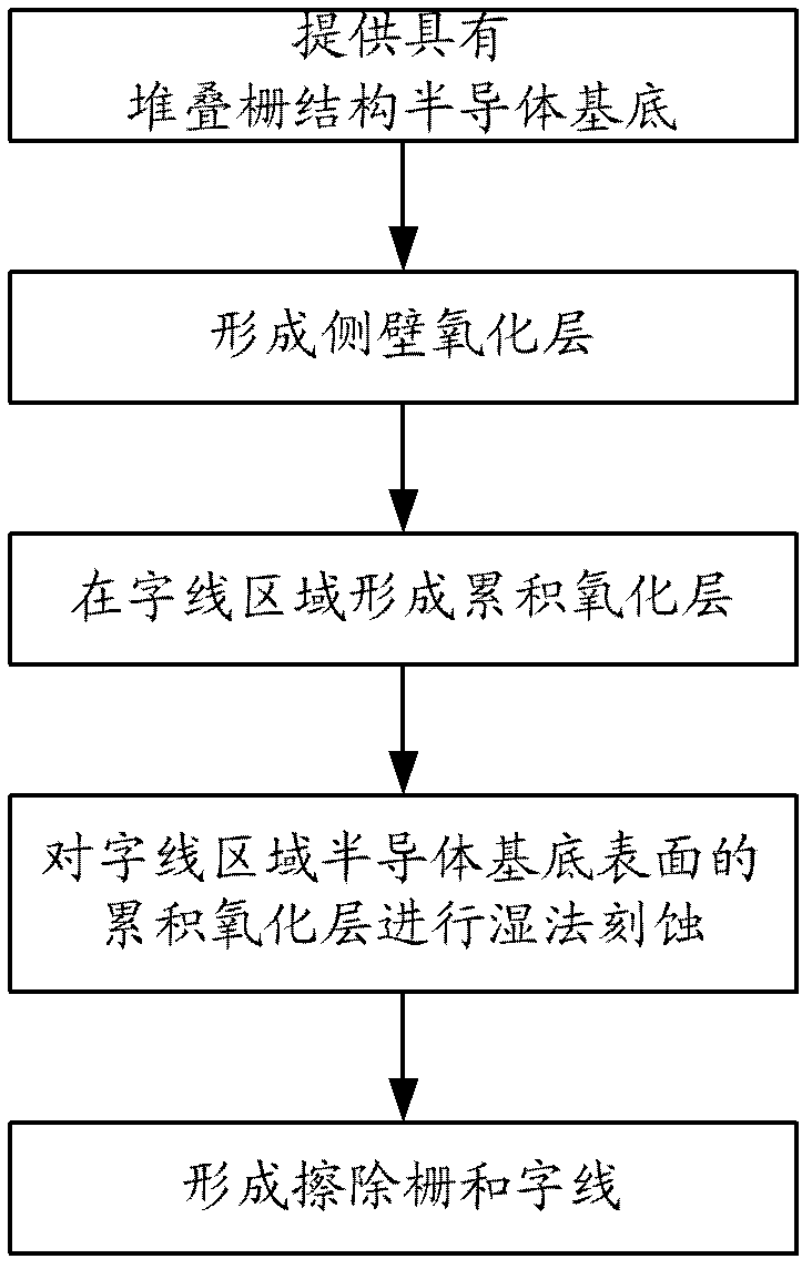
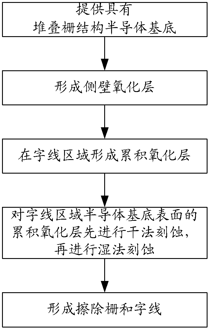
[0041] Such as figure 2 A method for manufacturing a split-gate flash memory unit of the present invention as shown, comprising:
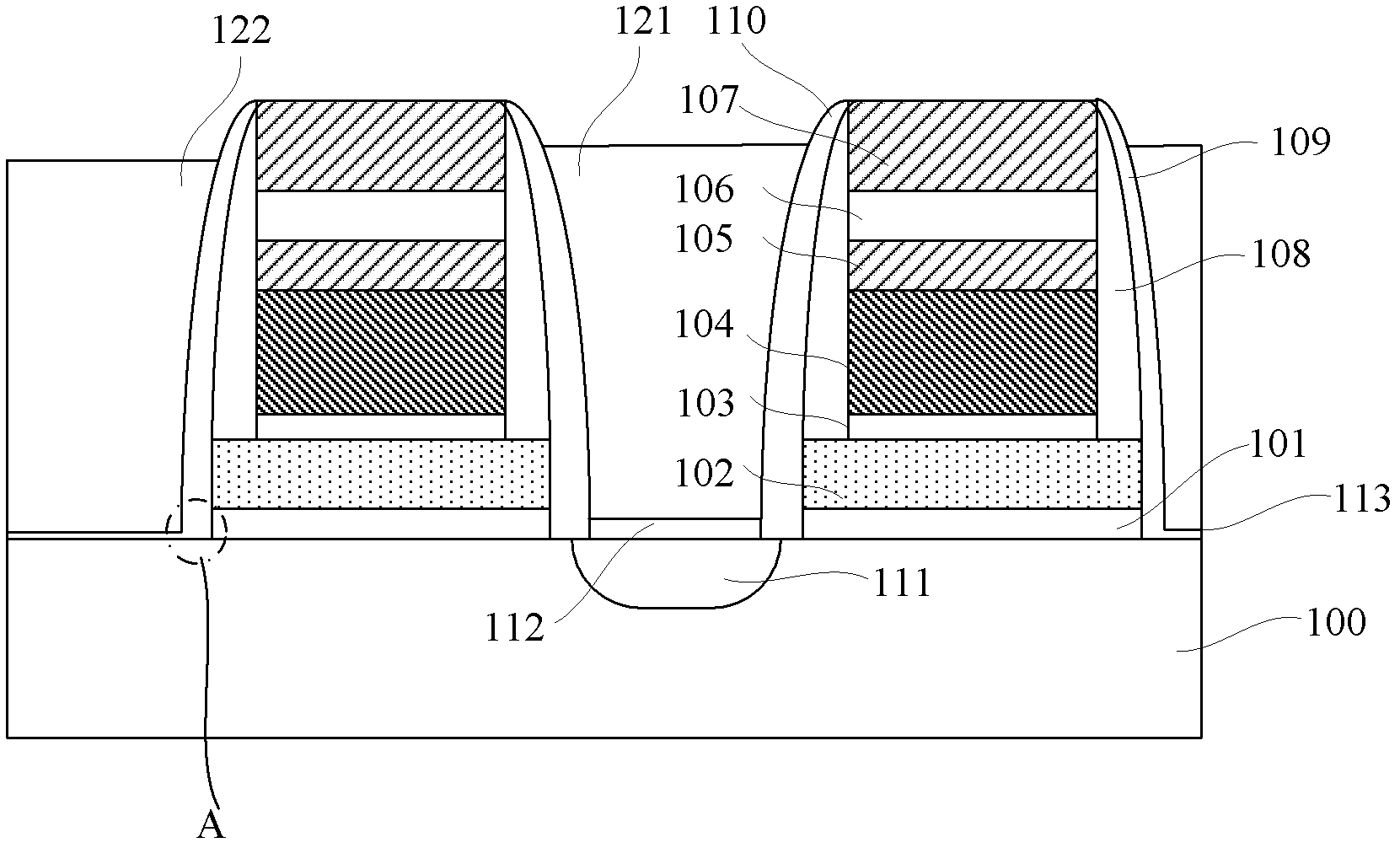
[0042]A semiconductor substrate is provided, on which a separated gate memory cell stack gate structure including a floating gate oxide layer, a floating gate, an intergate dielectric layer, a control gate, a control gate hard mask layer and a control gate sidewall layer is preformed and an erasing gate region and a word line region on one side of the stacked gate structure;
[0043] forming sidewall oxide layers on both sides of the stacked gate structure;
[0044] forming a high voltage oxide layer on the surface of the semiconductor substrate, the stacked gate structure, and the sidewall oxide layer;
[0045] blockin...
PUM
 Abstract
Description
Claims
Application Information
 - R&D Engineer
- R&D Manager
- IP Professional
- Industry Leading Data Capabilities
- Powerful AI technology
- Patent DNA Extraction
Browse by: Latest US Patents, China's latest patents, Technical Efficacy Thesaurus, Application Domain, Technology Topic.
© 2024 PatSnap. All rights reserved.Legal|Privacy policy|Modern Slavery Act Transparency Statement|Sitemap