
Array substrate, display device and driving method

A technology of an array substrate and a driving method, which is applied to static indicators, nonlinear optics, instruments, etc., can solve the problem that the horizontal electric field type liquid crystal display device cannot meet the requirements of wide viewing angle, etc. Effect

Active Publication Date: 2013-08-28
HEFEI BOE OPTOELECTRONICS TECH +1
View PDF6 Cites 7 Cited by
  • Summary
  • Abstract
  • Description
  • Claims
  • Application Information

AI Technical Summary

Problems solved by technology

[0003] Although the horizontal electric field type liquid crystal display device has the advantage of a larger viewing angle than the vertical electric field type liquid crystal display device, as the size of the liquid crystal display device becomes larger and larger, the horizontal electric field type liquid crystal display device cannot meet people's requirements for a wide viewing angle, especially It is a widescreen liquid crystal display device of 40 inches or more

Method used


Image

  • Array substrate, display device and driving method
  • Array substrate, display device and driving method
  • Array substrate, display device and driving method

Examples


Embodiment Construction

[0035] The following will clearly and completely describe the technical solutions in the embodiments of the present invention with reference to the accompanying drawings in the embodiments of the present invention. Obviously, the described embodiments are only some, not all, embodiments of the present invention.

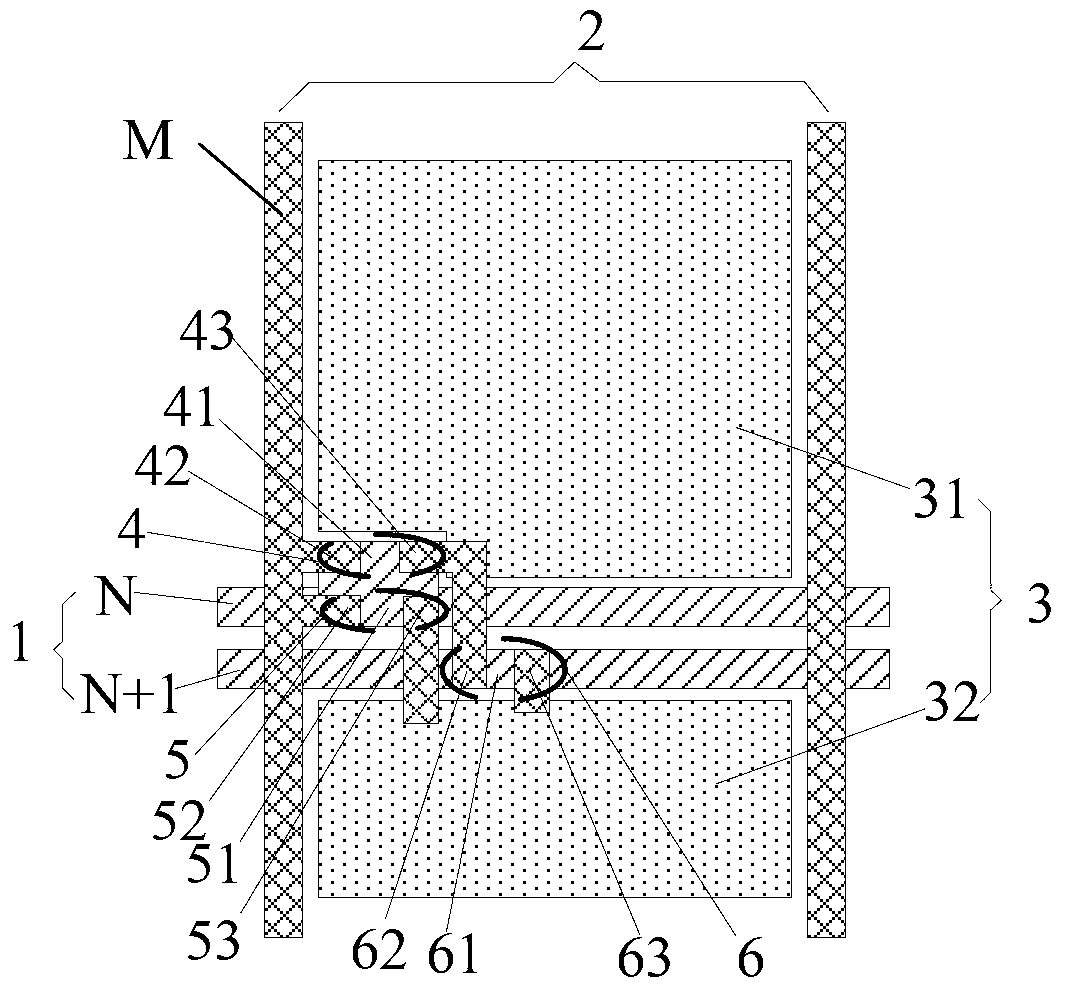
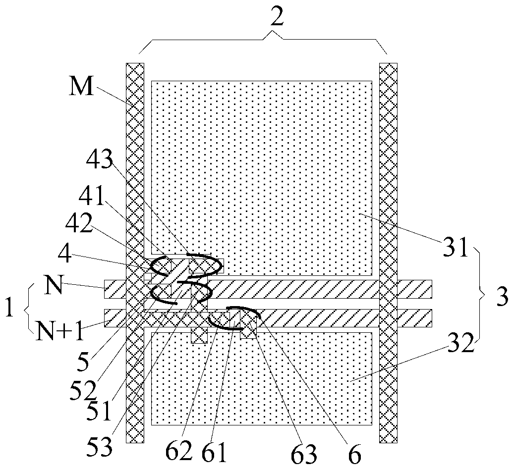
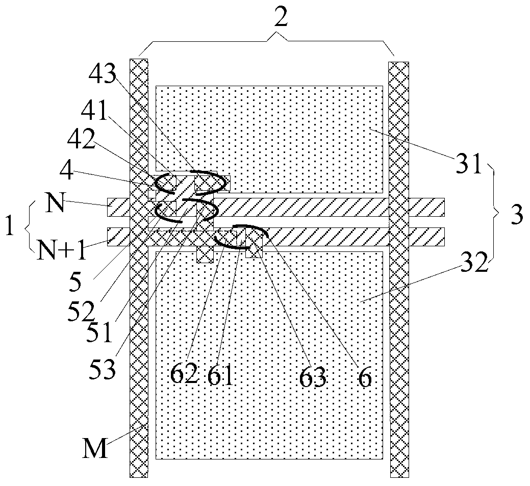
[0036] The invention provides an array substrate, such as figure 1 , figure 2 , image 3 shown, including:

[0037] A plurality of scanning signal lines 1, including the Nth scanning signal line and the N+1th scanning signal line, wherein N is a positive integer;

[0038] A plurality of data signal lines 2, including the Mth data signal line, where M is a positive integer;

[0039] The pixel unit 3 includes a first sub-pixel and a second sub-pixel, wherein the first sub-pixel includes a first pixel electrode 31, and the second sub-pixel includes a second pixel electrode 32;

[0040] The first switch unit includes a control terminal, an input terminal and an outp...


PUM


Abstract

The invention provides an array substrate, a display device and a driving method, and relates to the field of the display technology. The array substrate comprises an N scanning signal line, an N+1 scanning signal line, an M data signal line, a pixel unit, a first switch unit, a second switch unit and a third switch unit; the pixel unit comprises first sub-pixels and second sub-pixels; a control end of the first switch unit is electrically connected with the N scanning signal line, an input end of the first switch unit is electrically connected with the M data signal line, and an output end of the first switch unit is electrically connected with first pixel electrodes; a control end of the second switch unit is electrically connected with the N scanning signal line, an input end of the second switch unit is electrically connected with the M data signal line, and an output end of the second switch unit is electrically connected with second pixel electrodes; and a control end of the third switch unit is electrically connected with the N+1 scanning signal line, an input end of the third switch unit provides input signals, and an output end of the third switch unit is electrically connected with the second pixel electrodes. The array substrate, the display device and the driving method have the advantage that a visual angle of a liquid crystal display can be increased. The invention is applicable to designing and manufacturing display devices.

Description

technical field [0001] The present invention relates to the field of display technology, in particular to an array substrate, a display device and a driving method. Background technique [0002] A liquid crystal display device controls light transmittance through liquid crystals using an electric field to display images. Liquid crystal display devices are roughly classified into a vertical electric field driving type and a horizontal electric field driving type according to the direction of an electric field for driving liquid crystals. In the vertical electric field driven liquid crystal display device, a common electrode and a pixel electrode are arranged opposite to each other on the upper and lower substrates, and a vertical electric field is formed between the common electrode and the pixel electrode to drive the liquid crystal. In the horizontal electric field driven liquid crystal display device, a common electrode and a pixel electrode are arranged on the lower subs...

Claims


Application Information

Patent Timeline
Patent Type & Authority Applications(China)
IPC IPC(8): G02F1/1362G02F1/1368G02F1/133G09G3/36
CPCG02F1/13624G09G3/3659G02F1/134345
Inventor 姜清华李小和刘永邵贤杰李红敏
Owner HEFEI BOE OPTOELECTRONICS TECH
Learn More