Liquid crystal device and a method for producing it

a liquid crystal and device technology, applied in the field of liquid crystal devices, can solve the problems of non-satisfactory angular dependence of contrast, slow conventional nematic display with dielectric coupling to the electric field, and inability to optimize all important properties, etc., to achieve the effect of quick response of smectic c and increase field strength

Inactive Publication Date: 2001-06-28
ECSIBEO PPF1
View PDF0 Cites 22 Cited by
  • Summary
  • Abstract
  • Description
  • Claims
  • Application Information

AI Technical Summary

Benefits of technology

0037] 3. An important advantage of the invention is that is makes it possible to extend the advantages of in-plane molecule switching typical of e.g. SSFLCs, even including bistability, to conventional liquid crystal structures. As an example, a dynamic alignment layer according to the invention can be produced as a thin layer of smectic C* presenting a bistable, direct ferroelectric response to the applied electric field. A reversal of the field direction will result in a very quick response of the smectic C* layer. This the primary surface switching in response to the field reversal will be essentially as fast as the response of a conventional SSFLC. Due to (i) a coupling between the alignment layer and the surface molecules of the bulk layer, and (ii) a coupling between the surface molecules of the bulk layer and the molecules further into the bulk volume, the induced in-plane switching will be almost as fast as the primary surface switching. In other words, the invention makes it possible to electrically control a liquid crystal bulk layer in a very fast manner, without any specific requirement on the liquid crystal material, the thickness, the electrical response, etc of the bulk layer.
0038] 4. Many different types of liquid crystal materials can be used to implement the dynamic alignment layer.
0039] 5. Many different types of liquid crystal materials can be used to implement the bulk liquid crystal layer, such as a conventional non-chiral or chiral nematic or smectic in a twisted or non-twisted configuration.
0040] 6. The principle puts very few demands on the conventional liquid crystal and requires only a conventional and simple electrode structure.
0041] 7. The invention can be used to implement grey scale features. This can be performed by accomplishing a "two-step effect", if the liquid crystal material of the bulk layer also presents a direct response to the applied electric field. As an example, one could have the bulk layer formed by a nematic liquid crystal having a small positive dielectric anisotropy, and having a threshold voltage for dielectric switching above that of the dynamic alignment layer. Now, when the electric field strength is increased, the first switching (the primary surface switching) occurs e.g. when the voltage reaches a first threshold voltage for dynamic alignment layer. At this point, there is still no direct electrical coupling between the electric field and the bulk molecules. However, there will be an induced in-plane switching of the bulk molecules. This is the first step of the above-mentioned two-step effect. When increasing the field strength further, the voltage will exceed the threshold for dielectric switching within the bulk layer, leading to a homeotropic out-of-plane orientation of the nematic molecules. By the use of suitably orientated polarizers, the first step (induced in-plane switching) may extinguish light partly through the device, whereas the second step (the out-of-plane switching) may result in an essentially complete light blocking effect.
0042] The aforementioned and other embodiments and advantages of the invention can be seen from the claims and the description hereinbelow of some embodiments of the inventive device and the manufacturing thereof.

Problems solved by technology

Today, some liquid crystal displays are advantageous concerning some of the above-mentioned desired properties, but there exists no ideal display which is optimized concerning all of the important properties.
Conventional nematic displays with a dielectric coupling to the electric field are usually slow, and nearly all suffer from non-satisfactory angular dependence of the contrast due to the out-of-plane switching of the liquid crystal molecules.
Supertwist displays (twist angles of e.g. 270.degree.) have an improved steepness of the electro-optical characteristic, but they present longer switching times and not yet satisfying viewing angle dependence of the optical contrast.
These displays possess very small dependence of the optical contrast from the viewing angle, but the brightness and switching times are not satisfying.
A specific disadvantage of this display type is the requirement for an in-plane applied electric field which causes manufacturing problems.
Drawbacks of the surface stabilized ferroelectric liquid crystal displays (SSFLCD's) and the antiferroelectric liquid crystal displays include difficulties in orienting the smectic phase and maintaining the orientation of these phases.
Also, the power consumption is relatively high.
Another drawback is that the thickness of the liquid crystal layer must be limited, usually to about 2 .mu.m, in order to obtain the aimed-at coupling between an applied electric field and the spontaneous polarisation.
This requirement for small thickness of FLC devices make their production complicated, delicate and expensive.
A drawback of using photocontrolled command layers in order to change the liquid crystal alignment is the slow switching speed between the two states.
Another drawback is that the life time of the device is reduced due to UV-light degradation.

Method used


Image

  • Liquid crystal device and a method for producing it
  • Liquid crystal device and a method for producing it
  • Liquid crystal device and a method for producing it

Examples


example 1

Method for Preparation

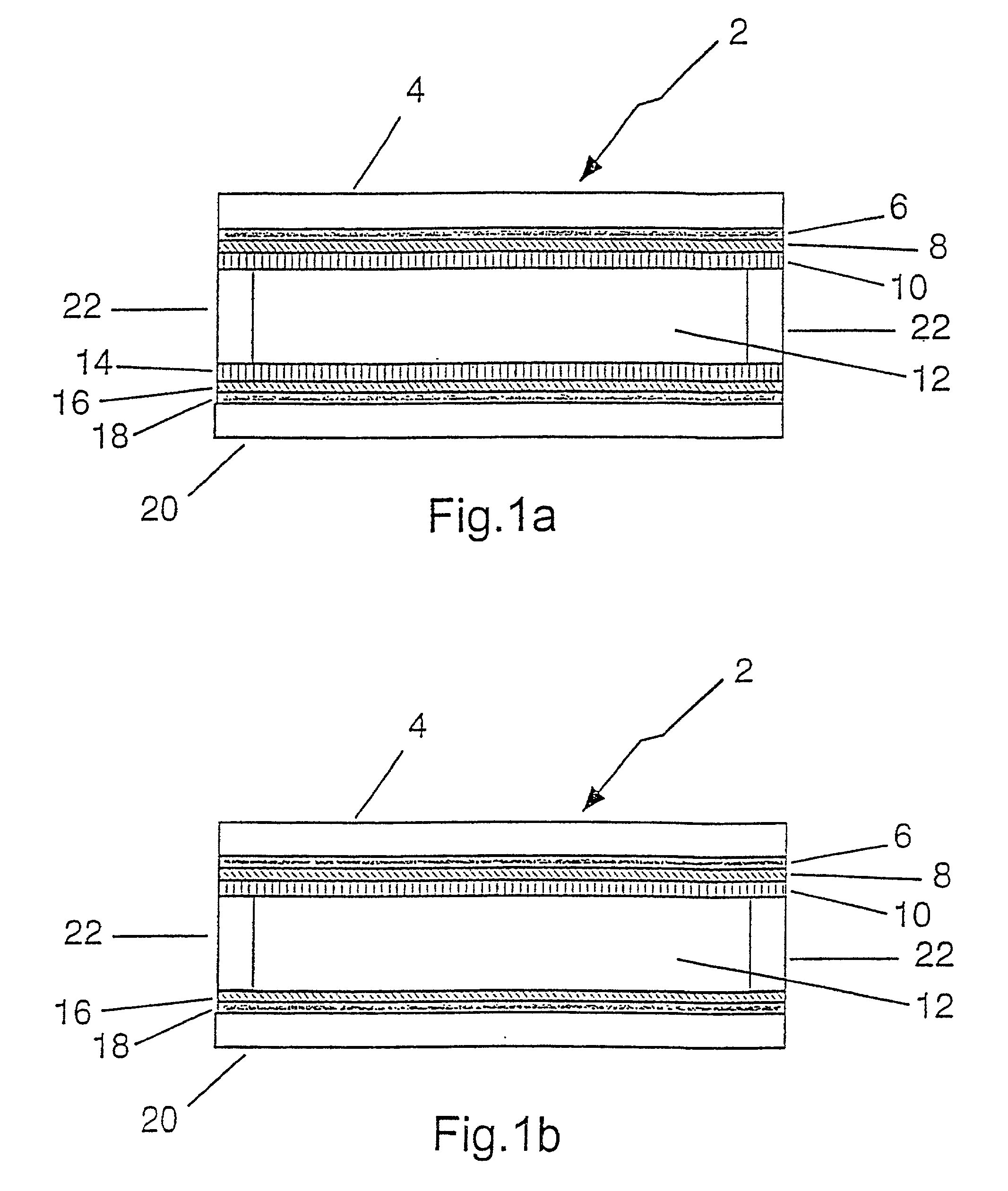
[0054] The following example describes a method for preparation of a chiral smectic surfaces forming e.g. the first dynamic alignment layer 10 in FIG. 1a.

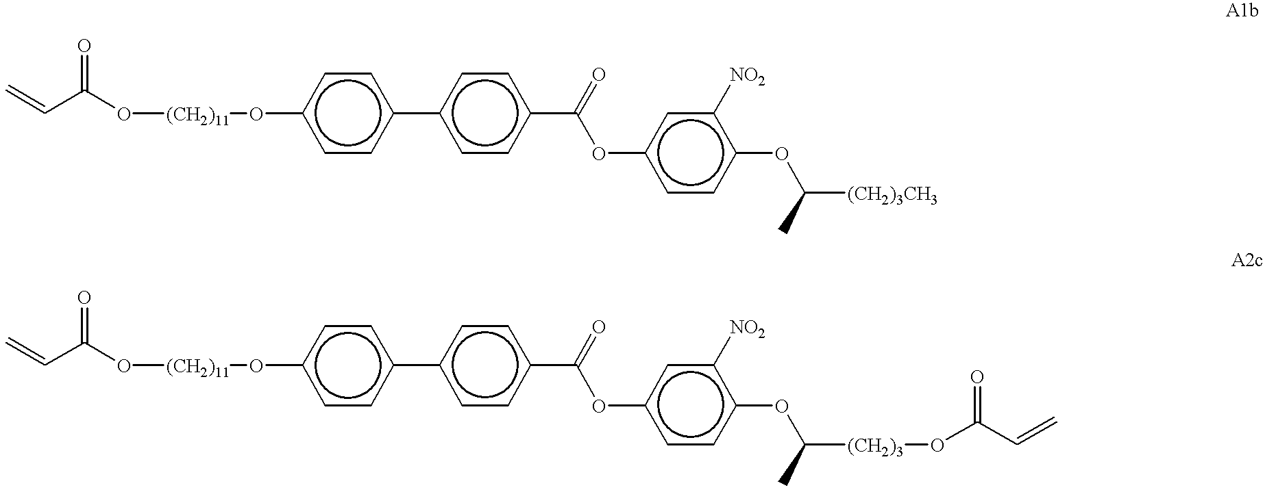
[0055] The inner surface of the glass substrate 4 is first covered with a transparent, conductive ITO film 6 and thereafter with a passive alignment layer 8 of buffed SiOx, evaporated at normal incidence. As well known, this passive alignment layer 8 gives a unidirectional planar alignment of most liquid crystal materials. In order to manufacture the dynamic surface alignment layer 10, the passive SiOx alignment layer 8 is now precoated with a thin layer of mixture of photoreactive liquid crystal monomers A1b / A2c (20 / 80% wt) and photoinitiator (usually added in a very small amount) by spinning a delute solution of this mixture in chloroform (about 10% wt). The structures of the monomers are the following: 1

[0056] As can be seen, A1b and A2c are monofunctional and bifunctional monomers, respectively, and both a...

example 2

Method for Preparation

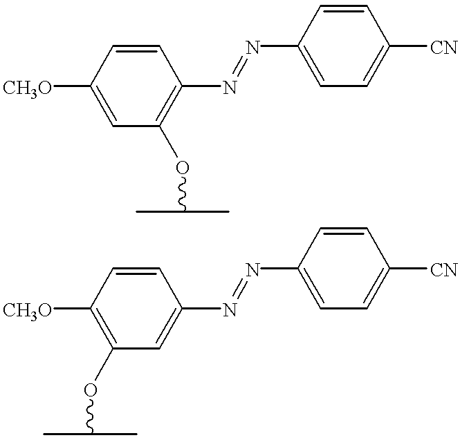
[0057] The following example also describes a method for preparation of a chiral smectic surface forming e.g. the first dynamic alignment layers 10 in FIG. 1a. The conductive ITO film 6 of glass substrate 4 is covered by a passive alignment layer 9 of photochromic material. This material is of the side-on type of attachment of azobenzene mieties at the ortho- or metha-position anchored onto silica surface through silylation, for instance. The molecular structure of such a material could be the following: 2

[0058] Then, the substrate is exposed to a linearly polarized UV-light which results in, as well known, a uniform planar alignment of the liquid crystal molecules in contact. Thereafter, the passive alignment layer is precoated by a photoreactive monomer A1b according to the procedure described in Example 1. After the polymerization, the molecules of this material seems to be uniformly oriented, well anchored to the passive alignment layer and insoluble in the...

example 3

Method for Preparation

[0059] In this example, the photoreactive monomer mixture A1b / A2c is mixed with a dichroic azo-dye or another photochromic material, which molecules can be aligned by a linearly polarized light. The wavelength used for the light controlled alignment of the dye molecules, and thus the alignment of the liquid crystal molecules in the first dynamic alignment layer 10, may differ from the wavelength of the light resulting in the photopolymerization of the photoreactive monomer mixture. Thus, the molecules of the dynamic alignment layers 10 will be first unidirectionally aligned by the linearly polarized light, and then photopolymerized.

In-plane Switching of Bulk Liquid Crystals

[0060] Some examples illustrating the induced in-plane switching according to the inventive principle will now be described.

[0061] The chiral surface mediated device (CSMD) used in the following examples consisted of two parallel electroded glass substrates 4 and 20 with a micron-size gap (sp...


PUM

PropertyMeasurementUnit
angleaaaaaaaaaa
apex angleaaaaaaaaaa
thicknessaaaaaaaaaa

Abstract

An electrooptic device (2), and the methods for manufacturing, including a liquid crystal material (12) disposed between electroded flat glass or polymer substrates (4, 20) which have been precoated with a e.g. a chiral smectic surface layer (10, 14) in such way that the surface layer is able to mediate switching of the liquid crystal (12) between different optical states. The chiral smectic surface layer can be a polymer, oligomer or monomer liquid crystal with paraelectric, ferroelectric, ferrielectric or antiferroelectric response, which is insoluble in the liquid crystal used for the bulk (12) between the electroded substrates (4, 20). the switchable surface director enforces a certain orientation of the optic axis in the bulk liquid crystal (12), which can be a conventional non-chiral or chiral nematic or smectic in a twisted or non-twisted configuration.

Description

[0001] The present invention generally relates to the field of liquid crystals. More specifically, the present invention relates to a liquid crystal device including a liquid crystal bulk layer, and a dynamic surface alignment layer interacting with the bulk layer for obtaining a preferred orientation of the surface director of the bulk layer. The invention also relates to a method for producing a liquid crystal device including such a dynamic surface alignment layer. Furthermore, the present invention relates to a method for accomplishing an in-plane switching in a liquid crystal bulk layer of a liquid crystal device.TECHNICAL BACKGROUND[0002] The operation of almost all liquid crystal devices is based on a direct coupling between, on the one hand, an electric field applied in a perpendicular direction across a liquid crystal bulk layer within the device and, on the other hand, an induced polarization of the liquid crystal layer (in dielectric or paraelectric liquid crystals) or a ...

Claims


Application Information

Patent Timeline
Patent Type & Authority Applications(United States)
IPC IPC(8): B32B7/02C09K19/02G02F1/13G02F1/1337G02F1/1347G02F1/141
CPCG02F1/133711G02F1/13471G02F1/141G02F2001/133726G02F2001/133769G02F1/133726G02F1/133769G02F1/1337
Inventor STEBLER, BENGTDEMUS, DIETRICHLAGERWALL, TORBJORNKOMITOV, LACHEZAR
Owner ECSIBEO PPF1
Why Eureka
Try Eureka