Flash memory programming using gate induced junction leakage current

a programming technique and flash memory technology, applied in static storage, digital storage, instruments, etc., can solve the problem of high power consumption of electron injection, achieve the effect of increasing the field strength of the substrate, increasing the generation of electron-hole pairs, and increasing the generation of pair

Active Publication Date: 2005-05-12
SANDISK TECH LLC
View PDF27 Cites 24 Cited by
  • Summary
  • Abstract
  • Description
  • Claims
  • Application Information

AI Technical Summary

Benefits of technology

[0044] Other factors may also be varied in order to optimize the method of the present invention. For example, the doping concentrations of substrate 10 and the active region 20 influence the bias current generation in the structure. In this respect, doping concentrations of the region 20 for an n-type region may be on the order of 1017-1020 atms / cm3 of an n-type impurity such as arsenic or phosphorous. Doping concentrations for the substrate 10 are a region implanted below floating gate FG and select gate SG and may be on the order of 1016-1018 atm / cm3 of an impurity such as boron. Greater doping concentrations of the p-type region will increase electron-hole pair generation, and hence the gate induced current in region 100. Another factor includes variance in the thickness of the select gate oxide 30 and floating gate oxide 25. Oxide thicknesses for the floating gate oxide 25 will generally be controlled by data retention characteristics for a given cell. In one embodiment, oxide thicknesses for floating gate oxide 25 may be in the range of approximately 80 to 90 angstroms, but may be thicker or thinner, depending on the application. Select gate oxide 30 may have a thickness different from that of the floating gate oxide, which may be in the range of about 20 angstroms to 200 angstroms. Thinner oxides at the select gate will increase the field strength in the substrate, again increasing pair generation. Voltage conditions may be applied in the following range: for the select gate SG, voltage may be in the range of 0 v to (−)3 v; for the control gate CG, voltage may be in the range of 7 v to 15 v; and for active region 20, voltage may be in the range of 3v-7.5 v.

Problems solved by technology

One disadvantage of channel hot electron injection is its high-power consumption.

Method used


Image

  • Flash memory programming using gate induced junction leakage current
  • Flash memory programming using gate induced junction leakage current
  • Flash memory programming using gate induced junction leakage current

Examples


Embodiment Construction

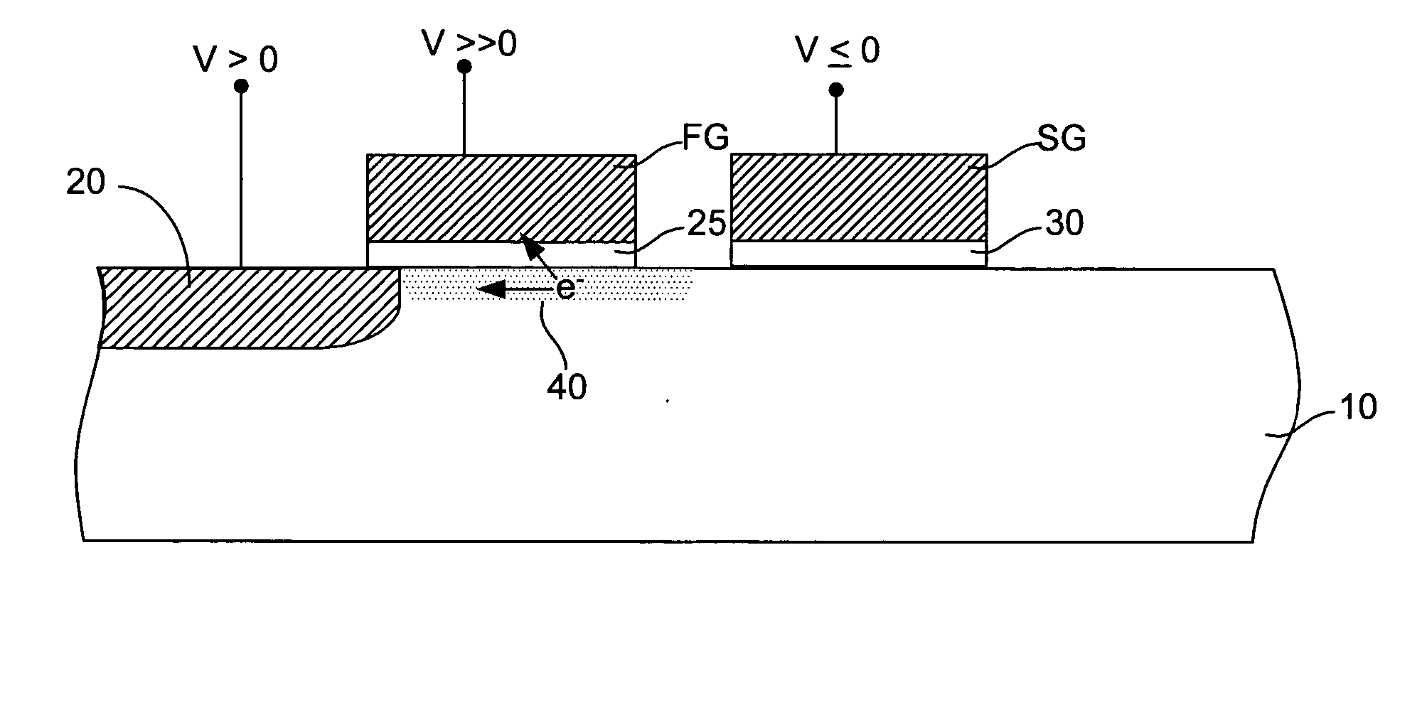
[0032]FIG. 1 is a cross-sectional diagram of an idealized non-volatile memory cell illustrating the principles of the present invention. It should be recognized that FIG. 1 shows a simplified representation of a basic cell, and omits certain details in order to more clearly present the invention. For example, the substrate and gate elements are illustrated with little detail of dielectrics and connection layers that exist in a practical implementation of the cell. However, it will be understood that appropriate dielectric and connection layers are to be included in a practical implementation of the structure.

[0033] Shown in FIG. 1 is a substrate 10 having a background doping concentration of, for example, a first impurity type, such as a p-type impurity. It should be understood that substrate 10 may represent a bulk substrate, or may represent an impurity well formed in a bulk substrate. It should also be understood that while the invention will be generally described with respect ...


PUM


Abstract

A method for programming a storage element and a storage element programmed using gate induced junction leakage current are provided. The element may include at least a floating gate on a substrate, an active region in the substrate, and a second gate adjacent to the floating gate. The method may include the steps of: creating an inversion region in the substrate below the floating gate by biasing the first gate; and creating a critical electric field adjacent to the second gate. Creating a critical electric field may comprise applying a first positive bias to the active region; and applying a bias less than the first positive bias to the second gate. The element further includes a first bias greater than zero volts applied to the active region and a second bias greater than the first bias applied to the floating gate and a third bias less than or equal to zero applied to the second gate. The first and third bias are selected to create leakage current in the substrate between the floating gate and the select gate.

Description

BACKGROUND OF THE INVENTION [0001] 1. Field of the Invention [0002] The present invention is directed to programming techniques for a storage element, and in particular, to programming non-volatile semiconductor memory devices. [0003] 2. Description of the Related Art [0004] Non-volatile semiconductor memory is popular for a number of uses, including cellular telephones, digital cameras, personal digital assistants, mobile computing devices, non-mobile computing devices and other devices. Electrical Erasable Programmable Read Only Memory (EEPROM) and flash memory are among the most popular non-volatile semiconductor memory types. [0005] Both EEPROM and flash memory utilize arrays of storage elements to store one or more bits of data per element. Each element generally includes a floating gate that is positioned above and insulated from a channel region and a semiconductor substrate. The floating gate is positioned between source and drain regions. A control gate may be provided over...

Claims


Application Information

Patent Timeline
Patent Type & Authority Applications(United States)
IPC IPC(8): G11C16/04G11C16/10
CPCG11C16/10G11C16/0425G11C16/04G11C16/30
Inventor LUTZE, JEFFREY W.PANG, CHAN-SUI
Owner SANDISK TECH LLC
Why Eureka
Try Eureka