Structure and method to improve short channel effects in metal oxide semiconductor field effect transistors

a technology of metal oxide semiconductor and short channel effect, applied in the direction of semiconductor devices, electrical apparatus, transistors, etc., can solve the problems of large side-wall junction capacitance, large vt roll-up, large junction leakage, etc., and achieve the effect of suppressing short channel effects and increasing control over short channel effects

Inactive Publication Date: 2008-05-29
IBM CORP +1
View PDF6 Cites 24 Cited by
  • Summary
  • Abstract
  • Description
  • Claims
  • Application Information

AI Technical Summary

Benefits of technology

[0010]The transistor structure further comprises buried isolation regions (e.g., buried nitride or oxide regions) within the semiconductor layer. These buried isolation regions can be below the level of the source / drain extension regions and can be between the deep source / drain regions and the channel region and, particularly, between the deep source / drain regions and the halo regions in order to suppress short channel effects. Buried isolation regions between the deep source / drain regions and channel region minimize drain induced barrier lowering (DIBL) as well as punch through. Additionally, because the deep source / drain regions and halo regions are separated by the buried isolation regions, side-wall junction capacitance and junction leakage are also minimized.

Problems solved by technology

However, it has been determined that such scaling has its limits because short channel lengths can lead to undesirable “short-channel effects” particularly in p-type field effect transistors.
However, the high halo dose that is used to control the short channel effects can also cause large junction leakage, large side-wall junction capacitance and large Vt roll-up.
Consequently, controlling these short channel effects has proven difficult to the point of limiting scaling of conventional MOSFETs.

Method used


Image

  • Structure and method to improve short channel effects in metal oxide semiconductor field effect transistors
  • Structure and method to improve short channel effects in metal oxide semiconductor field effect transistors
  • Structure and method to improve short channel effects in metal oxide semiconductor field effect transistors

Examples


Embodiment Construction

[0043]The embodiments of the invention and the various features and advantageous details thereof are explained more fully with reference to the non-limiting embodiments that are illustrated in the accompanying drawings and detailed in the following description. It should be noted that the features illustrated in the drawings are not necessarily drawn to scale. Descriptions of well-known components and processing techniques are omitted so as to not unnecessarily obscure the embodiments of the invention. The examples used herein are intended merely to facilitate an understanding of ways in which the embodiments of the invention may be practiced and to further enable those of skill in the art to practice the embodiments of the invention. Accordingly, the examples should not be construed as limiting the scope of the embodiments of the invention.

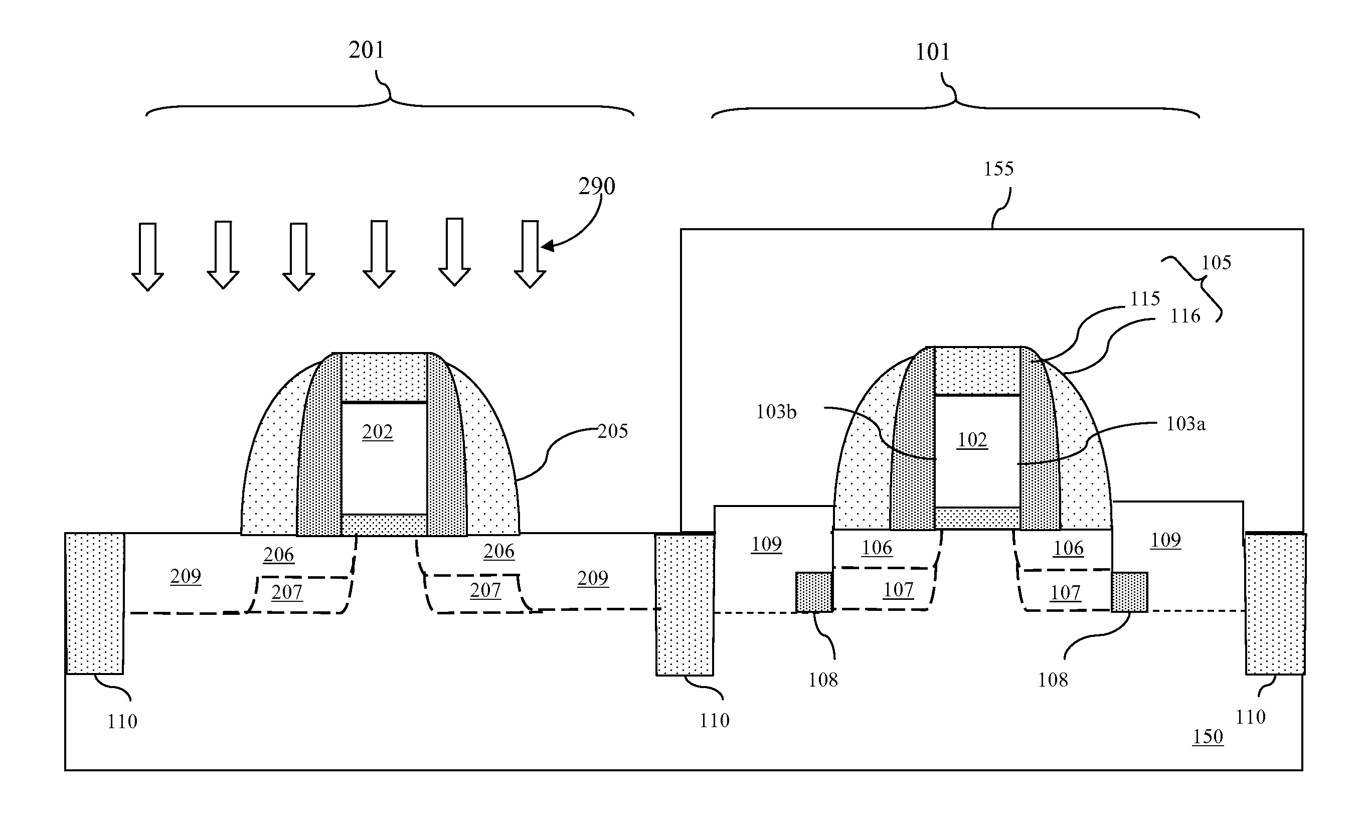
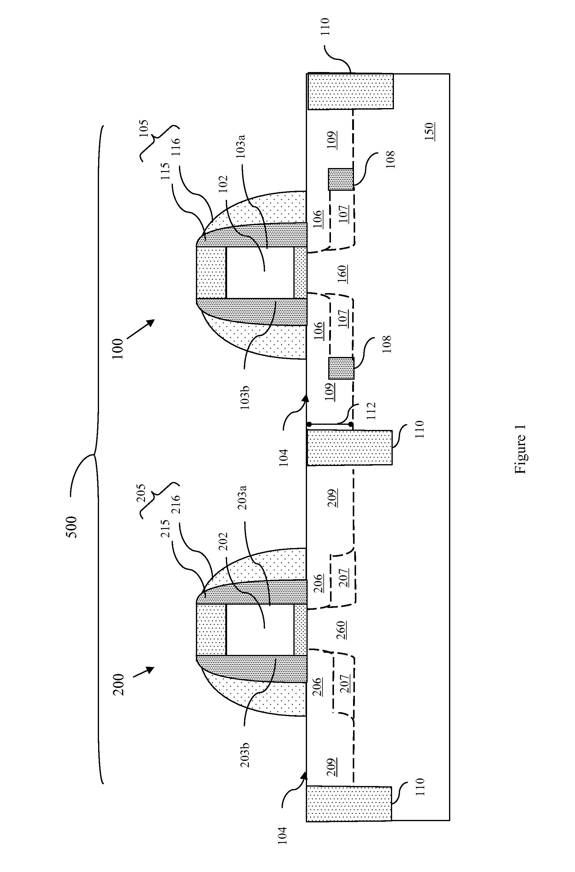
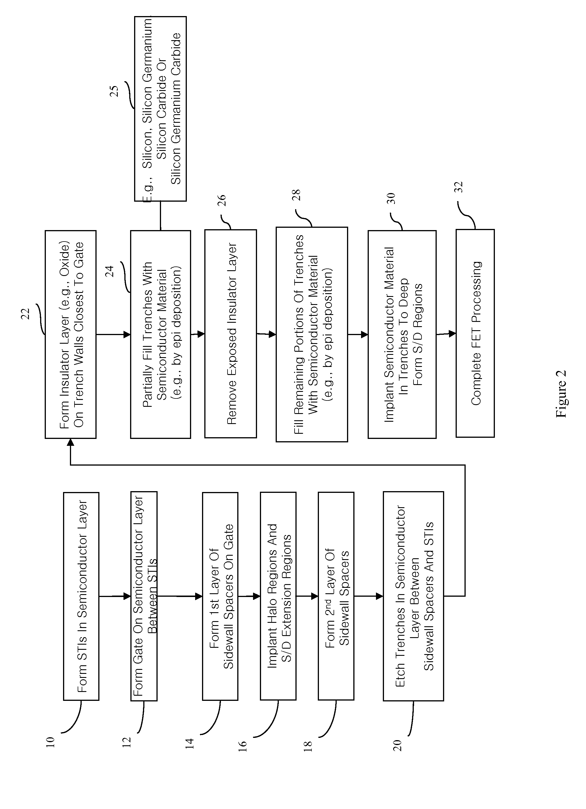
[0044]In view of the foregoing, referring to FIG. 1, disclosed herein are embodiments of both an improved metal oxide semiconductor field effect...


PUM


Abstract

Disclosed are embodiments of improved MOSFET and CMOS structures that provides for increased control over short channel effects. Also disclosed are embodiments of associated methods of forming these structures. The embodiments suppress short channel effects by incorporating buried isolation regions into a transistor below source / drain extension regions and between deep source / drain regions and the channel region and, particularly, between deep source / drain regions and the halo regions. Buried isolation regions between the deep source / drain regions and the channel region minimize drain induced barrier lowering (DIBL) as well as punch through. Additionally, because the deep source / drain regions and halo regions are separated by the buried isolation regions, side-wall junction capacitance and junction leakage are also minimized.

Description

BACKGROUND[0001]1. Field of the Invention[0002]The embodiments of the invention generally relate to semiconductor devices and, more particularly, to metal oxide semiconductor device structures with improved control over short channel effects.[0003]2. Description of the Related Art[0004]Over the past few decades numerous performance and economic advantages have been seen with semiconductor technology scaling. For example, size scaling of metal oxide semiconductor field effect transistor (MOSFET) has lead to decreased channel lengths and a corresponding increase in switching speeds (i.e., shorter channel lengths correspond to faster switching speeds). However, it has been determined that such scaling has its limits because short channel lengths can lead to undesirable “short-channel effects” particularly in p-type field effect transistors. These short channel effects include, but are not limited, variability in threshold voltage (Vt), excessive drain leakage currents, punch through, a...

Claims


Application Information

Patent Timeline
Patent Type & Authority Applications(United States)
IPC IPC(8): H01L27/088H01L21/04H01L29/78H01L21/77
CPCH01L21/823814H01L21/823878H01L29/0653H01L29/1083H01L29/7833H01L29/6656H01L29/66628H01L29/66636H01L29/165
Inventor CHEN, XIANGDONGPARK, DAE-GYUYOO, JAE-YOON
Owner IBM CORP
Why Eureka
Try Eureka