

Manufacturing method of semiconductor device
a manufacturing method and semiconductor technology, applied in the direction of semiconductor devices, electrical devices, transistors, etc., can solve the problems of junction leakage, difference in reaction rate, and one obstacle to the miniaturization of semiconductor devices, and achieve the effect of high performance of memory-logic-hybrid semiconductor devices
- Summary
- Abstract
- Description
- Claims
- Application Information
AI Technical Summary
Benefits of technology
Problems solved by technology
Method used
Image

Examples
first preferred embodiment
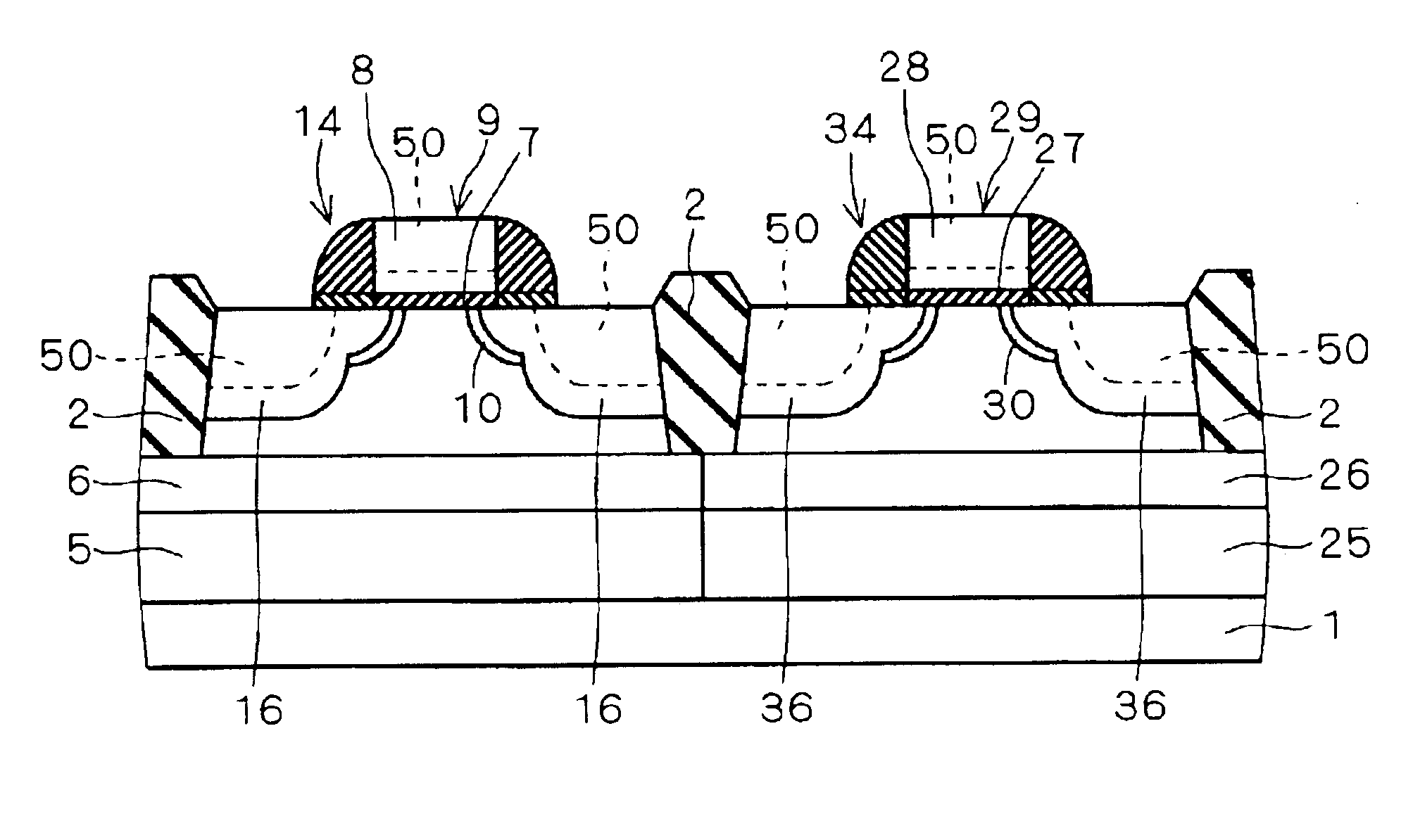
FIGS. 1 to 9, 12, and 13 are sectional views showing, in the order of the steps, a method of manufacturing a semiconductor device according to a first preferred embodiment of the present invention. This method will be described by referring to these drawings.
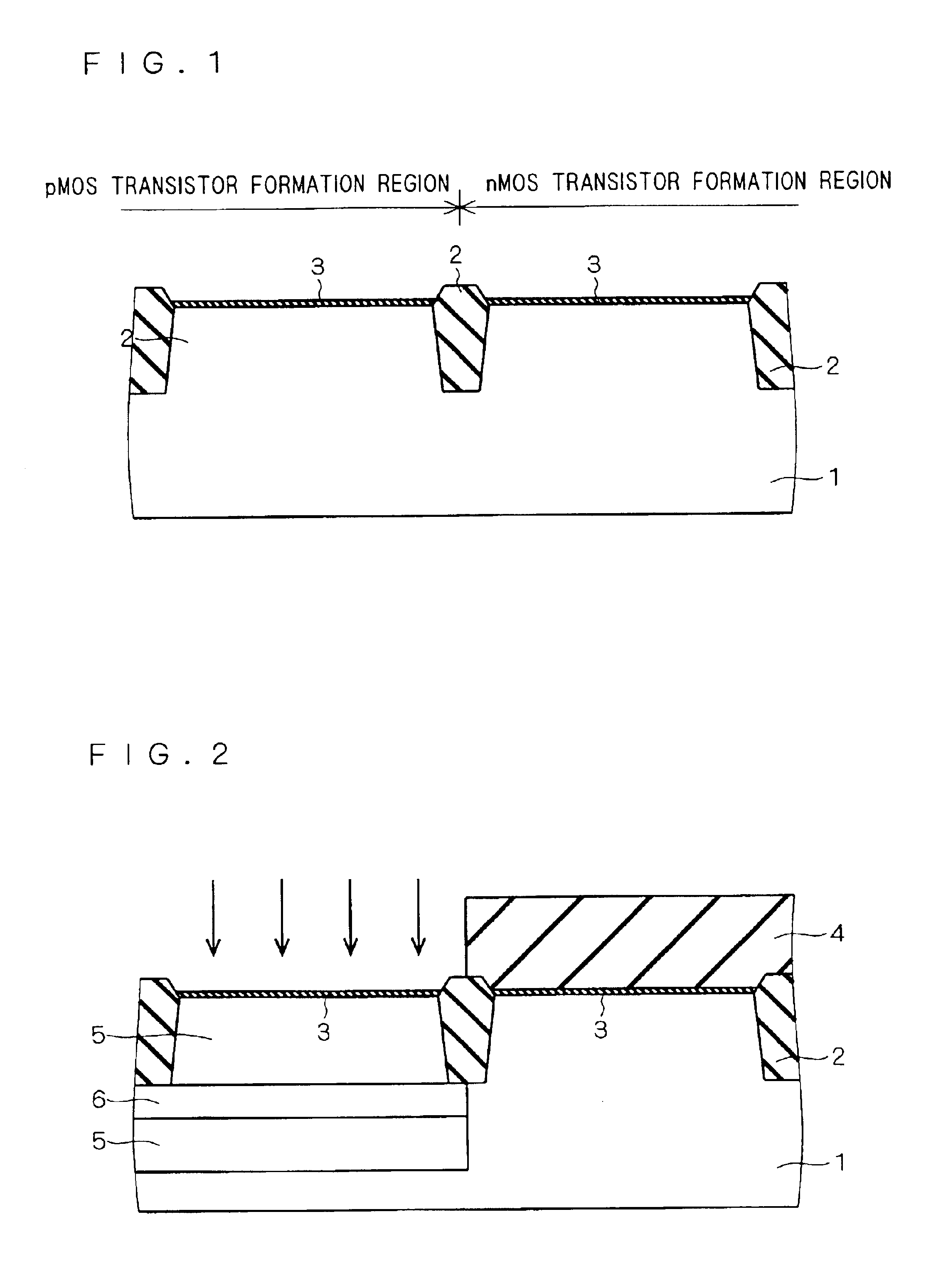
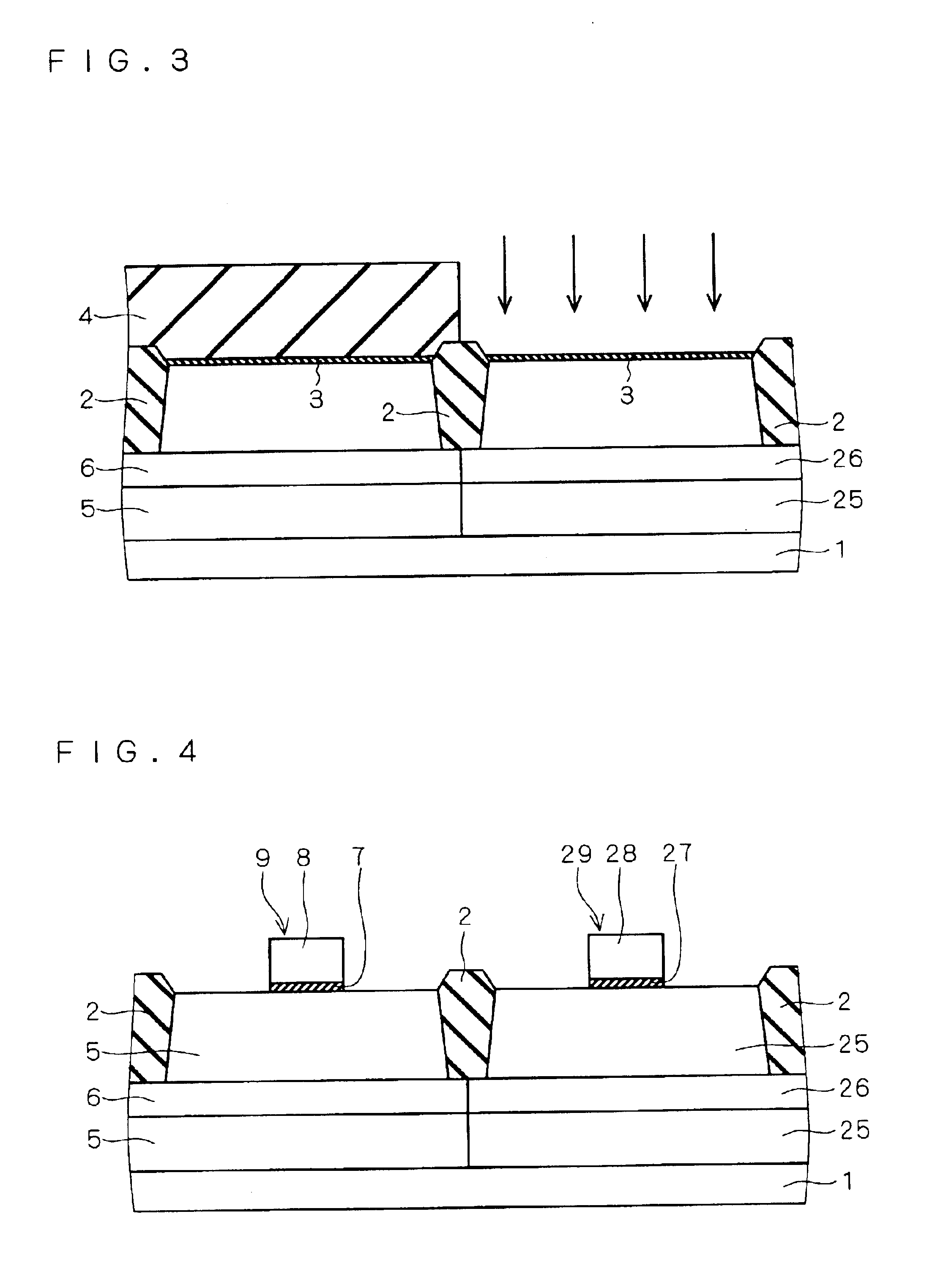
Referring now to FIG. 1, an element isolation insulating film 2 is formed in an upper surface of a semiconductor substrate 1 that is for example a p-type silicon substrate by a known LOCOS isolation technique or trench isolation technique. Then, a silicon oxide film 3 is formed on the semiconductor substrate 1 that is exposed.
The element isolation insulating film 2 is for example composed of a silicon oxide film, and it divides the semiconductor substrate 1 into a region where a p-channel MOS transistor is formed (hereinafter referred to as a “pMOS transistor formation region”) and a region where an n-channel MOS transistor is formed (hereinafter referred to as an “nMOS transistor formation region”).
Referring to FIG. 2, a photor...
second preferred embodiment
As previously described, when the source / drain region is made into silicide in the state that the semiconductor layer of the SOI substrate is thinned for miniaturizing the semiconductor device, there has been the problem that silicide grows greatly in the direction of the channel region underlying the gate electrode. To solve this problem, a second preferred embodiment of the present invention presents a manufacturing method that can prevent silicide formation reaction from extending to the channel region.
FIGS. 18 to 24 are sectional views showing, in the order of the steps, a method of manufacturing a semiconductor device according to the second preferred embodiment. This preferred embodiment is directed to a manufacturing method when a semiconductor layer and silicide film are formed at the same thickness.
Referring to FIG. 18, an SOI substrate 60 in which a support substrate 61, an insulating film 62, and a semiconductor layer 63 are laminated in the order named is prepared, and t...
PUM
 Abstract
Description
Claims
Application Information