Semiconductor device and method of manufacturing the same

a semiconductor and channel technology, applied in the direction of semiconductor devices, electrical devices, transistors, etc., can solve the problems of high barrier to solving, insufficient utilization of the merit of schottky source-drain which can inject high-speed carriers into channels, and difficulty in improving device performance relying only on micro-patterning, etc., to achieve effective suppression of short channel effect and junction leakage, improve performance, and increase the injection rate of carriers

Inactive Publication Date: 2008-01-03
KK TOSHIBA
View PDF12 Cites 24 Cited by
  • Summary
  • Abstract
  • Description
  • Claims
  • Application Information

AI Technical Summary

Benefits of technology

[0006] The present invention has been made in consideration of the above circumstances. It is an object of the present invention to provide a semiconductor device having a field effect transistor with a device structure which can achieve improvement of performance by increasing an injection rate of carriers while effectively suppressing a short channel effect and junction leakage, and a method of manufacturing the semiconductor device.
[0007] A semiconductor device according to an embodiment of the present invention comprises a field effect transistor including: a first semiconductor region of a first conductivity type having a surface portion on which a channel region is formed; a gate electrode formed on the channel region, a gate insulating film in between the gate electrode and the channel region; a source electrode and a drain electrode formed on both the sides of the channel region; second semiconductor regions of a second conductivity type formed between the source electrode and the channel region and between the drain electrode and the channel region to serve as extension regions of a source and a drain; third semiconductor regions of the second conductivity type formed between the source electrode and the first and second semiconductor regions and between the drain electrode and the first and second semiconductor regions and having an impurity concentration higher than that of the second semiconductor region; and side wall insulating films formed on both the side surfaces of the gate electrode, the side wall insulating films being separated from the source electrode and the drain electrode.
[0008] A method for producing the field effect transistor according to another embodiment of the present invention comprises: forming a gate electrode on a first semiconductor region of a first conductivity type, a gate insulating film in between, and side wall insulating films on both side surfaces of the gate electrode; ion-implanting an impurity in the first semiconductor region by using the gate electrode and the side wall insulating film as masks to form second semiconductor regions of a second conductivity type serving as extension regions of a source and a drain; forming second side wall insulating films on both side surfaces of the side wall insulating film; and siliciding a part of the second semiconductor region of the second conductivity type to a region deeper than the second semiconductor region to form a source electrode and a drain electrode, and forming third semiconductor regions of the second conductivity type having an impurity concentration higher than that of the second semiconductor region in interfaces between the source electrode and the first and second semiconductor regions and between the drain electrode and the first and second semiconductor regions by segregation from silicide.
[0009] A method for producing the field effect transistor according to still another embodiment of the present invention comprises: forming a ga

Problems solved by technology

However, as micro patterning advanced, a technical barrier to be solved becomes high at the same time.
For this reason, improvement of device performance relying only to micro patterning is very difficult.
However, a device structure using a conventional Schottky source-drain has the following problem.
That is, the merit of

Method used


Image

  • Semiconductor device and method of manufacturing the same
  • Semiconductor device and method of manufacturing the same
  • Semiconductor device and method of manufacturing the same

Examples


first embodiment

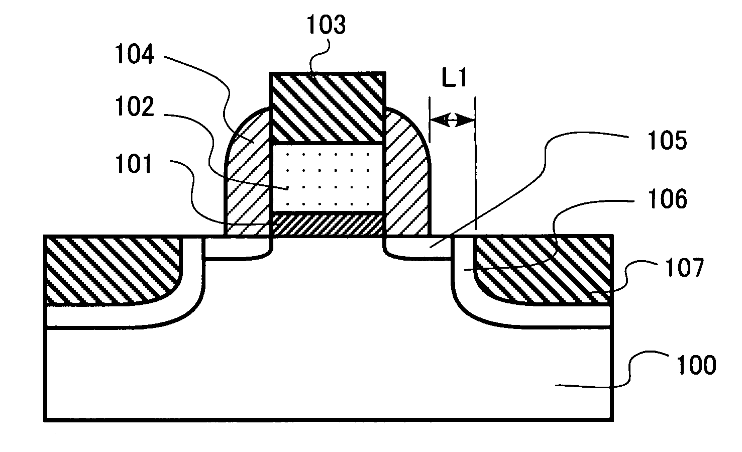
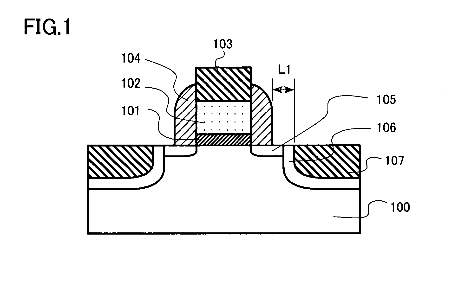
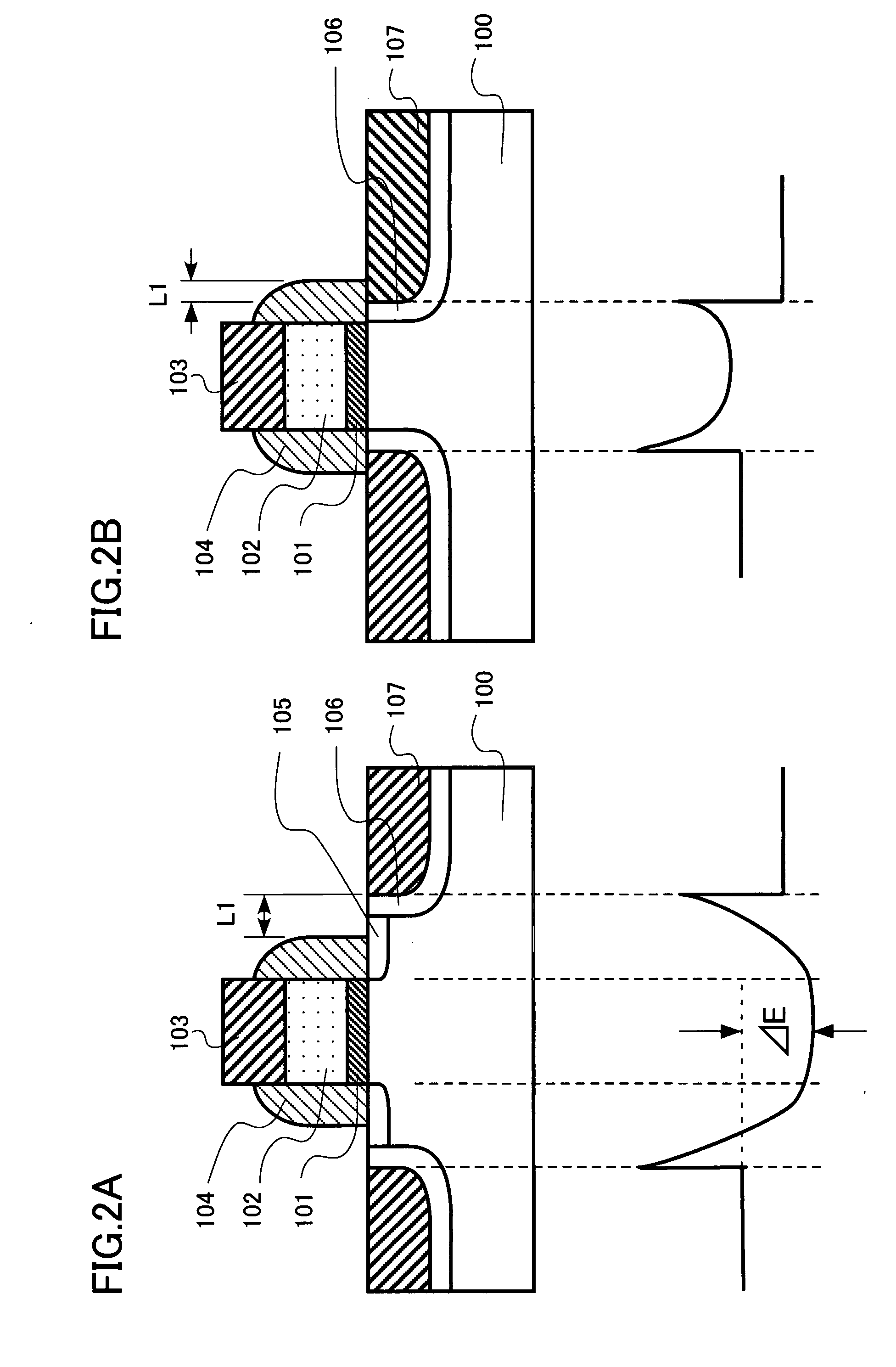
[0026]FIG. 1 is a sectional view showing an device structure of a MIS field effect transistor according to a first embodiment.

[0027] A polysilicon gate electrode 102 is formed on a p-type silicon substrate (first semiconductor region) 100 a gate insulating film 101 in between. A gate silicide 103 is formed on the polysilicon gate electrode 102. In this case, the gate electrode 102 is made of polysilicon. However, a metal gate structure in which the polysilicon gate electrode 102 and the gate silicide 103 are replaced by a single metal layer may be employed.

[0028] On both the side surfaces of the gate electrodes 102 and 103, a gate side wall insulating film 104 constituted by a silicon nitride film is formed. Source and drain regions are formed in the silicon substrate 100 to interpose a channel region under the polysilicon gate electrode 102. The source and drain regions are constituted by, an n-type extension diffusion layer (second semiconductor region) 105 using, for example, A...

second embodiment

[0072]FIG. 24 is a cross-sectional view showing an device structure of a MIS field effect transistor according to a second embodiment of the present invention. Since the MIS field effect transistor is the same as that in the first embodiment except that an HALO diffusion layer (fourth semiconductor region) 201 is formed, a description thereof will be omitted.

[0073] The HALO diffusion layer 201 is a p-type region the impurity type of which is the same as that of a silicon substrate 100, and has an impurity concentration higher than that of the silicon substrate 100 as a characteristic feature. The field effect transistor according to the embodiment includes the HALO diffusion layer 201 to obtain the operation and effect of the first embodiment and to achieve improvement of a roll-off characteristic.

third embodiment

[0074]FIG. 25 is a cross-sectional view showing an device structure of a MIS field effect transistor according to a third embodiment of the present invention. Since the MIS field effect transistor according to the third embodiment is the same as that of the first embodiment except that an n+-type deep diffusion layer (fifth semiconductor region) 301 is formed, a description thereof will be omitted.

[0075] The n+-type deep diffusion layer 301 is formed between an n+-type high-concentration impurity layer 106 and the silicon substrate 100, and has a thickness of, for example, about 50 nm.

[0076] The field effect transistor according to the embodiment includes the n+-type deep diffusion layer 301 to obtain the operation and effect of the first embodiment and to achieve a considerable reduction in junction leakage from the source-drain bottom portion.

[0077] Due to the presence of the n+-type high-concentration impurity layer 106, the n+-type deep diffusion layer 301 can be made shallow...


PUM


Abstract

A semiconductor device which can effectively suppress a short channel effect and junction leakage is provided. A semiconductor device includes a field effect transistor. The field effect transistor includes a first semiconductor region of a first conductivity type, a gate electrode formed on a gate insulating film, and source and drain electrodes. The field effect transistor also includes second semiconductor regions of a second conductivity type. The field effect transistor further includes third semiconductor regions of the second conductivity type having an impurity concentration higher than that of the second semiconductor region and formed between the source electrode and the first and second semiconductor regions and between the drain electrode and the first and second semiconductor regions, and side wall insulating films formed on both the side surfaces of the gate electrode. The source electrode and the drain electrode are separated from the side wall insulating films.

Description

CROSS-REFERENCE TO RELATED APPLICATION [0001] This application is based upon and claims the benefit of priority from the prior Japanese Patent Application No. 2006-171593 filed on Jun. 21, 2006 in Japan, the entire contents of which are incorporated herein by reference. FIELD OF THE INVENTION [0002] The present invention relates to a semiconductor device and a method of manufacturing the same, and more particularly, to a semiconductor device having a MIS field effect transistor the source and drain portions of which are improved and a method of manufacturing the same. BACKGROUND OF THE INVENTION [0003] To advance the performance of a semiconductor integrated circuit, the performance of a field effect transistor serving as a constituent device must be advanced. For advancing the device performance, scaling down of the device is effective. For this reason, device performance has been improved by scaling down the device by micro patterning. However, as micro patterning advanced, a tech...

Claims


Application Information

Patent Timeline
IPC IPC(8): H01L29/78H01L21/336
CPCH01L29/1045H01L29/1083H01L29/6659H01L29/6653H01L29/665
Inventor KINOSHITA, ATSUHIROKOGA, JUNJI
Owner KK TOSHIBA
Why Eureka
Try Eureka