Storage device unit restoring device and method and storage device system comprising device

A memory system and memory technology, applied in the field of memory systems, can solve problems such as errors

Inactive Publication Date: 2013-09-11
SAMSUNG ELECTRONICS CO LTD
View PDF0 Cites 29 Cited by
  • Summary
  • Abstract
  • Description
  • Claims
  • Application Information

AI Technical Summary

Problems solved by technology

[0003] Recently, as the process of manufacturing semiconductor chips such as dynamic random access memory (DRAM) has become finer, errors are more likely to occur during the manufacturing process
Also, even if no errors are detected during the initial testing phase, errors may occur during chip operation

Method used


Image

  • Storage device unit restoring device and method and storage device system comprising device
  • Storage device unit restoring device and method and storage device system comprising device
  • Storage device unit restoring device and method and storage device system comprising device

Examples


Embodiment Construction

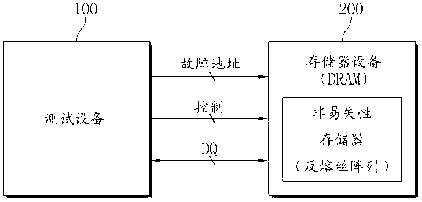
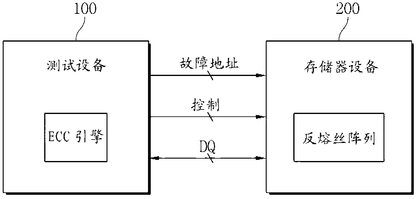
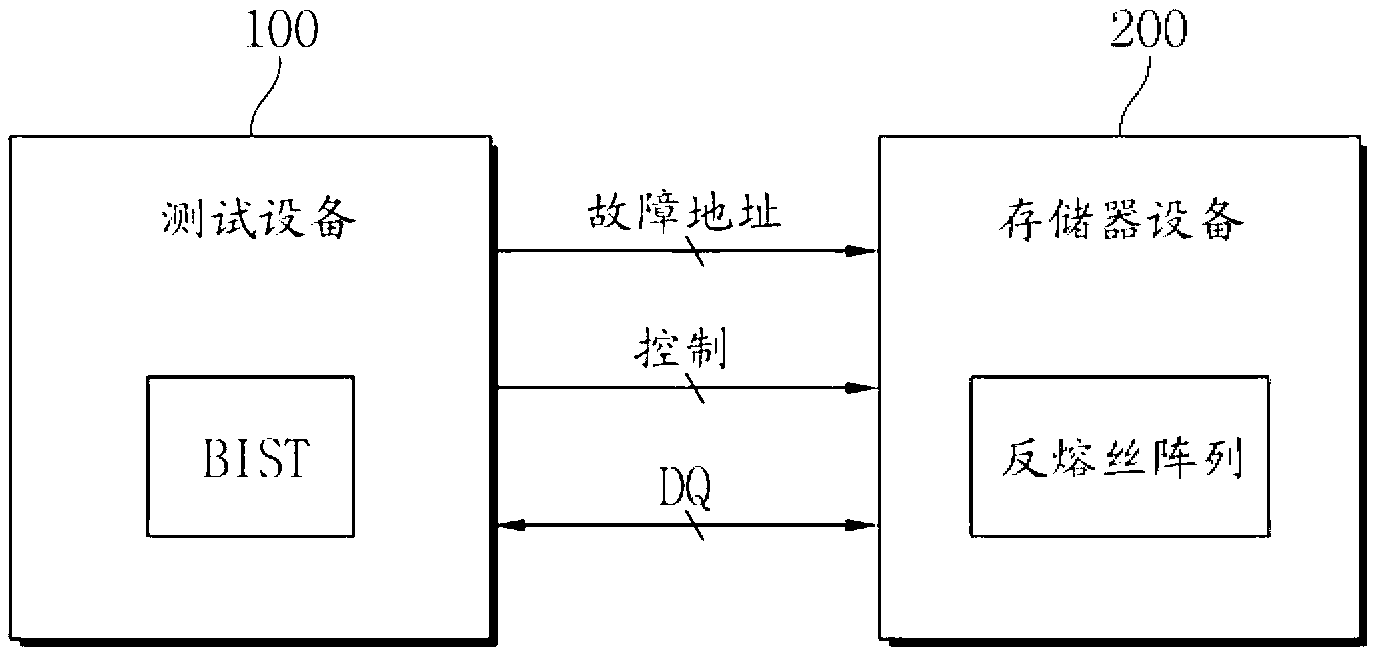
[0080] Various embodiments will now be described more fully with reference to the accompanying drawings in which some embodiments are shown. However, the inventive concepts may be embodied in different forms and should not be construed as limited to the embodiments set forth herein. Rather, these embodiments are provided so that this disclosure will be thorough and complete, and will fully convey the inventive concept to those skilled in the art. In the drawings, like reference numerals denote like elements, and the size and relative sizes of layers and regions may be exaggerated for clarity.

[0081] The terminology used herein is for the purpose of describing particular embodiments only and is not intended to limit the inventive concepts. As used herein, the singular forms "a", "an" and "the" are intended to include the plural forms as well, unless the context clearly dictates otherwise. It will also be understood that when used in this specification, the terms "comprise" ...


PUM


Abstract

A method and a device for restoring the storage device unit in a storage device system are disclosed. A testing device detects a fault address by testing storage device equipment according to a test order and temporarily stores the fault address in a fault address storage device (FAM). According to a fault address transmitting mode, the fault address is transmitted to the storage device equipment and is temporarily stored in a temporary fault address storage device of the storage device equipment and is then stored in an anti-fuse array which is used as a nonvolatile storage device. To ensure the reliability of data, stored data is read for verifying data and a verification result is transmitted to the testing device through data pins in a serial or parallel manner.

Description

technical field [0001] Embodiments of the inventive concept relate to a memory system, and more particularly, to a method and apparatus for repairing a memory cell by testing a memory device including a nonvolatile memory device using a test device, and a system including the same. Background technique [0002] Semiconductor chips are manufactured according to the semiconductor manufacturing process, and then tested using test equipment in the form of wafers, dies, or packages. Through testing, defective parts or defective chips can be picked out. When some memory cells of the semiconductor chip are defective, the semiconductor chip is repaired by restoring such defective memory cells. [0003] Recently, as the process of manufacturing semiconductor chips such as dynamic random access memory (DRAM) has become finer, errors are more likely to occur during the manufacturing process. Also, even if no errors are detected during the initial testing phase, errors may occur durin...

Claims


Application Information

Patent Timeline
Patent Type & Authority Applications(China)
IPC IPC(8): G11C29/42G11C29/44
Inventor 孙敎民宋镐永黄祥俊金澈孙东贤
Owner SAMSUNG ELECTRONICS CO LTD
Why Eureka
Try Eureka