Preparation method of aperiodic wideband response electro-optic modulator

An electro-optic modulator, non-periodic technology, applied in nonlinear optics, instruments, optics, etc., can solve problems such as high cost hindering commercial development and mass production

Inactive Publication Date: 2013-09-18
SHANGHAI JIAO TONG UNIV
View PDF8 Cites 4 Cited by
  • Summary
  • Abstract
  • Description
  • Claims
  • Application Information

AI Technical Summary

Problems solved by technology

However, there are accidental factors in the optical power tolerance and long-term stability of this prior art, and its high cost hinders commercial development and mass production

Method used


Image

  • Preparation method of aperiodic wideband response electro-optic modulator
  • Preparation method of aperiodic wideband response electro-optic modulator
  • Preparation method of aperiodic wideband response electro-optic modulator

Examples


Embodiment 1

[0034] In this embodiment, an electro-optic modulator with aperiodic broadband response is prepared, and the steps are as follows:

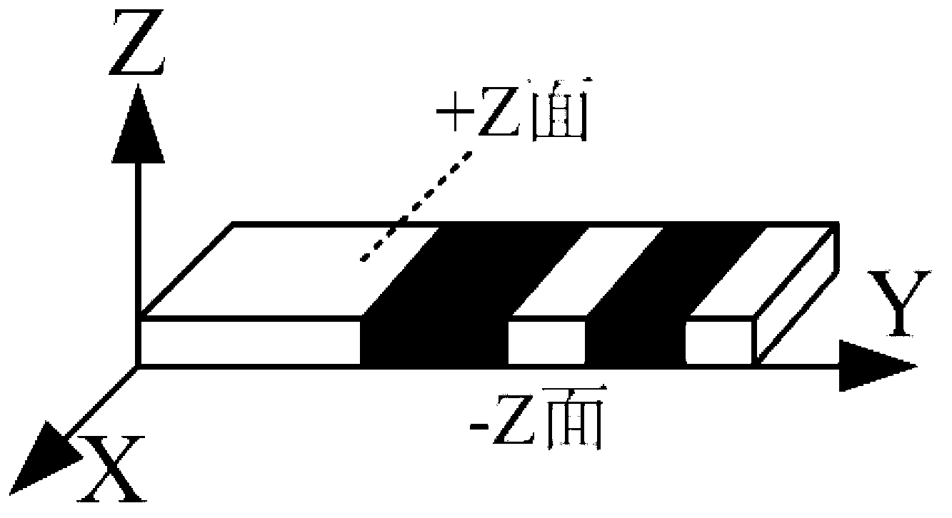
[0035] (1) if figure 2 As shown, the selected size is 65mm (length L) × 10mm (width W) × 0.5mm (thickness H). That is, a Z-cut pure lithium niobate wafer with a thickness of 0.5mm, the ±Z planes are all polished, where the +Z plane is parallel to the horizontal plane and faces the positive direction of the Z-axis, and the -Z plane is parallel to the horizontal plane and faces the negative direction of the Z-axis;

[0036] (2) Set the wavelength of the incident light as continuous light of λ=1053nm, set the driving frequency center frequency as 3GHz, and set the response bandwidth as 0.6GHz;

[0037] (3) Select the domain area width of a single active sample d=55μm, considering the convenience of packaging in the subsequent steps, select the total number of active domains N=1000, that is, the length of the action of light waves and microwaves is L...

Embodiment 2

[0055] This embodiment is an aperiodic broadband response electro-optic modulator prepared by applying the method of Example 1. The electro-optic modulator is under the condition of the target response bandwidth, that is, at f m = Under any frequency microwave drive between 2.7GHz and 3.3GHz, the spectrum of the incident light can be broadened Δf n = 2f m θ, where: Δf n is the spectral spread, f m is the microwave frequency, and θ is the spectral modulation degree.


PUM

PropertyMeasurementUnit
lengthaaaaaaaaaa
widthaaaaaaaaaa
thicknessaaaaaaaaaa

Abstract

A preparation method of an aperiodic wideband response electro-optic modulator comprises the following steps: selecting a ferroelectric single domain crystal; selecting the widths d of the electric domains of a single acting sample in a to-be-prepared crystal and the number N of total electric domains, and obtaining the polarization direction of each electric domain by computing to acquire the arrangement sequences of the positive electric domains and the negative electric domains so as to form an aperiodic optical superlattice; performing room-temperature electric-field polarization to the structure of the aperiodic optical superlattice; preparing a running-wave electrode on the +Z surface of the aperiodic optical superlattice in an evaporation manner, connecting a high-frequency resistor to the tail part of the running-wave electrode in series, and arranging a polarizer before the crystal of the aperiodic optical superlattice to form the electrooptical modulator. The preparation method provides abundant reciprocal lattice vectors by virtue of the aperiodicity of the optical superlattice to compensate the phase velocity difference between a microwave and an optical wave with different frequencies so as to force the electro-optic modulator to acquire a modulating action with a consistent effect under the drive of different-frequency microwaves applicable to a bandwidth.

Description

technical field [0001] The invention relates to a preparation method in the field of electro-optic modulation, in particular to a preparation method of an aperiodic broadband response electro-optic modulator. Background technique [0002] With the modern information society's requirements for high-speed and large-capacity communication systems, optoelectronic technology has developed rapidly. Using photons that are 1000 times higher than the electronic communication carrier frequency as the communication carrier frequency overcomes the limitations of microelectronics technology and achieves the purpose of more accurate, efficient and long-distance transmission of information. Therefore, electro-optic modulators, as "bridges" that closely combine electrons and photons, have been vigorously developed. [0003] Optical modulation is the process of loading an electrical signal onto a light wave and making the light wave measurable, such as phase, frequency, amplitude, and polar...

Claims


Application Information

Patent Timeline
Patent Type & Authority Applications(China)
IPC IPC(8): G02F1/035
Inventor 李俊陈险峰邹芸邓学伟
Owner SHANGHAI JIAO TONG UNIV
Why Eureka
Try Eureka