Semiconductor substrate and manufacturing method thereof

A semiconductor and manufacturing method technology, applied in the field of semiconductor substrate manufacturing, can solve problems such as bottom silicon pollution, unavoidable energy loss, and damage to semiconductor device functions, so as to achieve good shielding effect and enhanced heat dissipation effect

Active Publication Date: 2013-11-13
INNOGRATION SUZHOU
View PDF4 Cites 13 Cited by
  • Summary
  • Abstract
  • Description
  • Claims
  • Application Information

AI Technical Summary

Problems solved by technology

However, this method will have the following problems: first: increasing the resistivity of the bottom silicon 11 means that the single crystal purity of the bottom silicon is required to be very high, which imposes high requirements on the manufacturing process of the silicon wafer; 2. The semiconductor thin layer 13 on the bottom silicon 11 will inevitably be doped with various impurities in the subsequent processing technology. In these doping processes, the bottom silicon will inevitably be polluted, reducing the bottom The purity of silicon; third, high-purity single crystal silicon means that the entire device needs to be processed at high temperature for various processes, and high temperature operation has certain limitations for some semiconductor devices, and even destroys the function of semiconductor devices ; Fourth, although the increase in the current rate of the bottom silicon is realized in many difficulties, this increase still cannot avoid the loss of energy
[0008] In order to ensure the high resistivity characteristics of the bottom silicon, complex high-temperature (>1000°C) treatment is required for the bottom silicon. This high-temperature treatment will face the risk of destroying the polycrystalline structure for the polysilicon shielding layer. In addition, compared with polysilicon Single crystal silicon is more susceptible to the influence of doping impurities on the conductivity, so the risk of contamination in the subsequent semiconductor processing process is still unavoidable

Method used


Image

  • Semiconductor substrate and manufacturing method thereof
  • Semiconductor substrate and manufacturing method thereof
  • Semiconductor substrate and manufacturing method thereof

Examples


Embodiment Construction

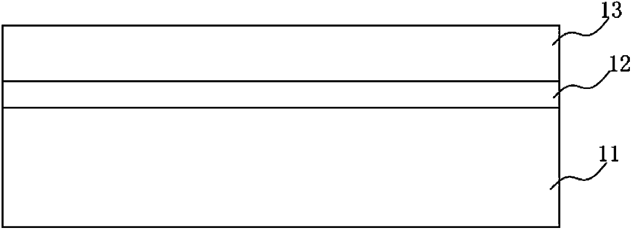
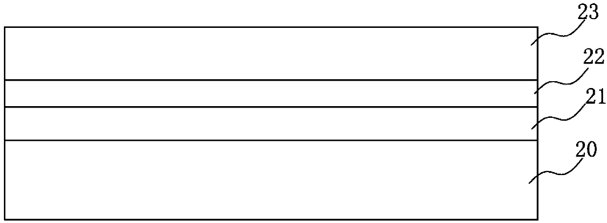
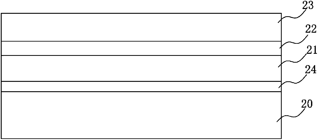
[0040] As mentioned in the background technology, in order to reduce the leakage loss caused by the bottom silicon when the existing silicon-on-insulator semiconductor substrate is used in some high-frequency devices, some high-resistivity single-crystal silicon supports are specially designed However, this not only increases the cost of SOI technology, but also does not really solve the problem. No matter how much the resistivity of single crystal silicon increases, there will always be problems of leakage current and power loss. In Soitec's technology, polysilicon is used as the shielding layer, although it can reduce the leakage current in the bottom silicon, but this method of improving the overall resistivity always faces the problems of impurity pollution and high temperature in processing engineering. In addition, in the existing semiconductor substrates, since the supporting substrate at the bottom is an insulating substrate, semiconductor devices fabricated on such sem...


PUM

PropertyMeasurementUnit
electrical resistivityaaaaaaaaaa
thicknessaaaaaaaaaa
electrical resistivityaaaaaaaaaa

Abstract

The invention discloses a semiconductor substrate and a manufacturing method thereof. The semiconductor substrate comprises a support substrate as well as a polycrystalline silicon layer, a first oxide layer and a semiconductor layer which are sequentially located on the support substrate, wherein the support substrate is a heavy doped type silicon substrate; the specific resistance of the support substrate is in 10 <-3> omega.cm by means of the impurity doping concentration of the support substrate; and the polycrystalline silicon layer similarly can adopt conductive or insulated polycrystalline silicon. The semiconductor substrate structure adopts a design thought opposite to SOI (silicon on insulator), the silicon substrate of the support substrate is designed into a heavy doped conductive substrate, and a grounding effect is achieved through the conductive substrate, so that not only are the problems of leakage current and power loss solved, but also more electrode connection schemes and heat dissipation solving schemes of a semiconductor device further can be provided.

Description

technical field [0001] The invention relates to the field of semiconductor substrate fabrication, in particular to a substrate with a highly doped semiconductor-on-conductor structure. Background technique [0002] SOI (Silicon-On-Insulator) refers to silicon on insulator, which can realize the dielectric isolation of devices in integrated circuits. The unique buried insulating layer of SOI structure separates the device from the substrate, eliminating the latch-up effect of bulk silicon CMOS circuits. Integrated circuits made of SOI structure devices have the advantages of small parasitic capacitance, high speed, high integration, simple process, and small short channel effect. [0003] See figure 1 , the traditional SOI type substrate structure usually includes: bottom silicon 11 (i.e. support layer), the bottom silicon 11 is usually made of silicon single crystal with high resistivity; oxide layer 12, usually silicon oxide material; and semiconductor material The thin l...

Claims


Application Information

Patent Timeline
Patent Type & Authority Applications(China)
IPC IPC(8): H01L21/84H01L27/12H01L23/34
Inventor 马强
Owner INNOGRATION SUZHOU
Why Eureka
Try Eureka