A liquid crystal display panel

A liquid crystal display panel, liquid crystal technology, applied in the direction of static indicators, etc., can solve problems such as unfavorable afterimages after shutdown, time delay, incomplete discharge of pixels, etc., and achieve the effect of solving afterimages after shutdown

Active Publication Date: 2016-03-16
NANJING CEC PANDA LCD TECH
View PDF4 Cites 0 Cited by
  • Summary
  • Abstract
  • Description
  • Claims
  • Application Information

AI Technical Summary

Problems solved by technology

[0006] When the size of the LCD panel is getting larger and the resolution is getting higher and higher, it becomes more and more difficult to quickly discharge each pixel in the LCD panel after the power is turned off, and it is easy to cause the LCD panel to be far away from the gate driver. The pixels on the IC side are not fully discharged, even if the high voltage (VGH) is output to all gate channels when the power is turned off, there will still be so-called power-off afterimages, such as image 3 Shown is a schematic diagram of afterimage after shutdown of the LCD panel
[0007] At present, the problem of afterimage after power off is solved by controlling the signal XAO. Under normal circumstances, the XAO signal is at a high level. When the circuit detects that the power is turned off, the XAO signal will change from a high level to a low level. The XAO signal is controlled by the circuit. The board is connected to the IC of the gate driver through COF (ChipOnFlex, or, ChipOnFilm, often called chip-on-film) and glass traces. After the IC of the gate driver receives the XAO signal, it must convert XAO to a higher level, and then Output a high voltage (VGH) to all gate channels (Gatechannels), such a transmission and conversion process, there is a certain time delay, which is not conducive to solving the afterimage after shutdown

Method used


Image

  • A liquid crystal display panel
  • A liquid crystal display panel
  • A liquid crystal display panel

Examples


Embodiment Construction

[0025] Below in conjunction with accompanying drawing and specific embodiment, further illustrate the present invention, should be understood that these embodiments are only for illustrating the present invention and are not intended to limit the scope of the present invention, after having read the present invention, those skilled in the art will understand various aspects of the present invention Modifications in equivalent forms all fall within the scope defined by the appended claims of this application.

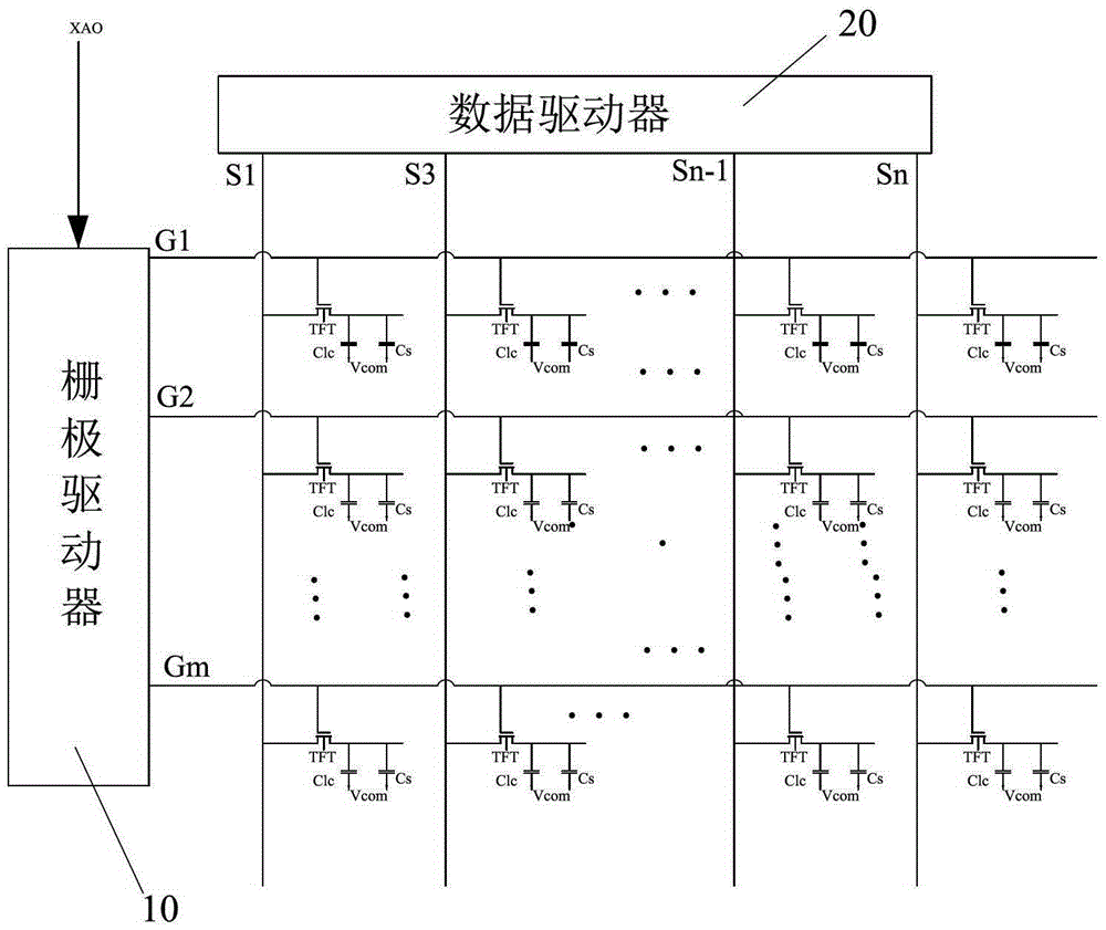
[0026] Figure 4 Shown is a schematic diagram of the circuit driving of the liquid crystal display panel of the present invention. The liquid crystal display panel includes an array substrate and a color filter substrate arranged oppositely, and a liquid crystal sandwiched between the array substrate and the color filter substrate. The color filter substrate is provided with a color filter Electrodes; the array substrate is provided with a display area and a non-display ...


PUM


Abstract

The invention provides a liquid crystal display panel. A plurality of second thin film transistors TFT are arranged on a non-display area away from the side of a grid driver, and each second thin film transistor TFT corresponds to each scanning line of a display area. Second source electrodes of the second thin film transistors TFT are connected with the corresponding scanning lines of the display area, second grid electrodes of the second thin film transistors TFT are connected with corresponding second drain electrodes, and the second grid electrode ends of all the second thin film transistors TFT are connected. A circuit board is externally connected with the liquid crystal display panel, the second grid electrode ends of all the second thin film transistors are connected onto the circuit board through wires. By means of the liquid crystal display panel, the plurality of thin film transistors are added in the non-display area, the circuit board is externally connected with liquid crystal display panel, a circuit is arranged on the circuit board, signals on the circuit are input into an inner thin film transistor, and the thin film transistors controlling opening or closing of the non-display area is opened, so that pixel voltage of the display area can be discharged fast, and the problem of residual image in shutdown can be solved.

Description

technical field [0001] The invention relates to a liquid crystal display panel used for solving afterimages stored when the liquid crystal display is turned off. Background technique [0002] When the power supply of the liquid crystal display panel is cut off, since all external voltages are quickly returned to zero, the source and gate drivers stop operating, and the pixel voltage of the liquid crystal display panel is discharged only by the Ioff (leakage current) of the TFT. Since the Ioff is very small, Therefore, the pixel voltage cannot be fully discharged, and a large amount of charge remains in the pixel. This phenomenon is called power-off afterimage. [0003] figure 1 It is a schematic diagram of circuit driving of an existing liquid crystal display panel. The liquid crystal display panel includes an array substrate and a color filter substrate arranged opposite to each other, and a liquid crystal sandwiched between the array substrate and the color filter substra...

Claims


Application Information

Patent Timeline
Patent Type & Authority Patents(China)
IPC IPC(8): G02F1/133
Inventor 卢建宏
Owner NANJING CEC PANDA LCD TECH
Why Eureka
Try Eureka