Supercharge Your Innovation With Domain-Expert AI Agents!

Method for manufacturing light emitting diode

A technology of light-emitting diodes and manufacturing methods, applied in the direction of electrical components, circuits, semiconductor devices, etc., can solve the problems of poor installation adaptability and single installation method, and achieve the effect of strong installation adaptability

Inactive Publication Date: 2013-12-04
广东艾力森数码电器有限公司
View PDF2 Cites 0 Cited by
  • Summary
  • Abstract
  • Description
  • Claims
  • Application Information

AI Technical Summary

Problems solved by technology

However, for the light-emitting diode made by this method, because its two electrodes are arranged on the bottom of the package and only its bottom surface is exposed, when this light-emitting diode is installed, generally only the bottom surface of the electrode exposed can be attached to the circuit board. Single installation method, poor installation adaptability

Method used


Image

  • Method for manufacturing light emitting diode
  • Method for manufacturing light emitting diode
  • Method for manufacturing light emitting diode

Examples


Embodiment Construction

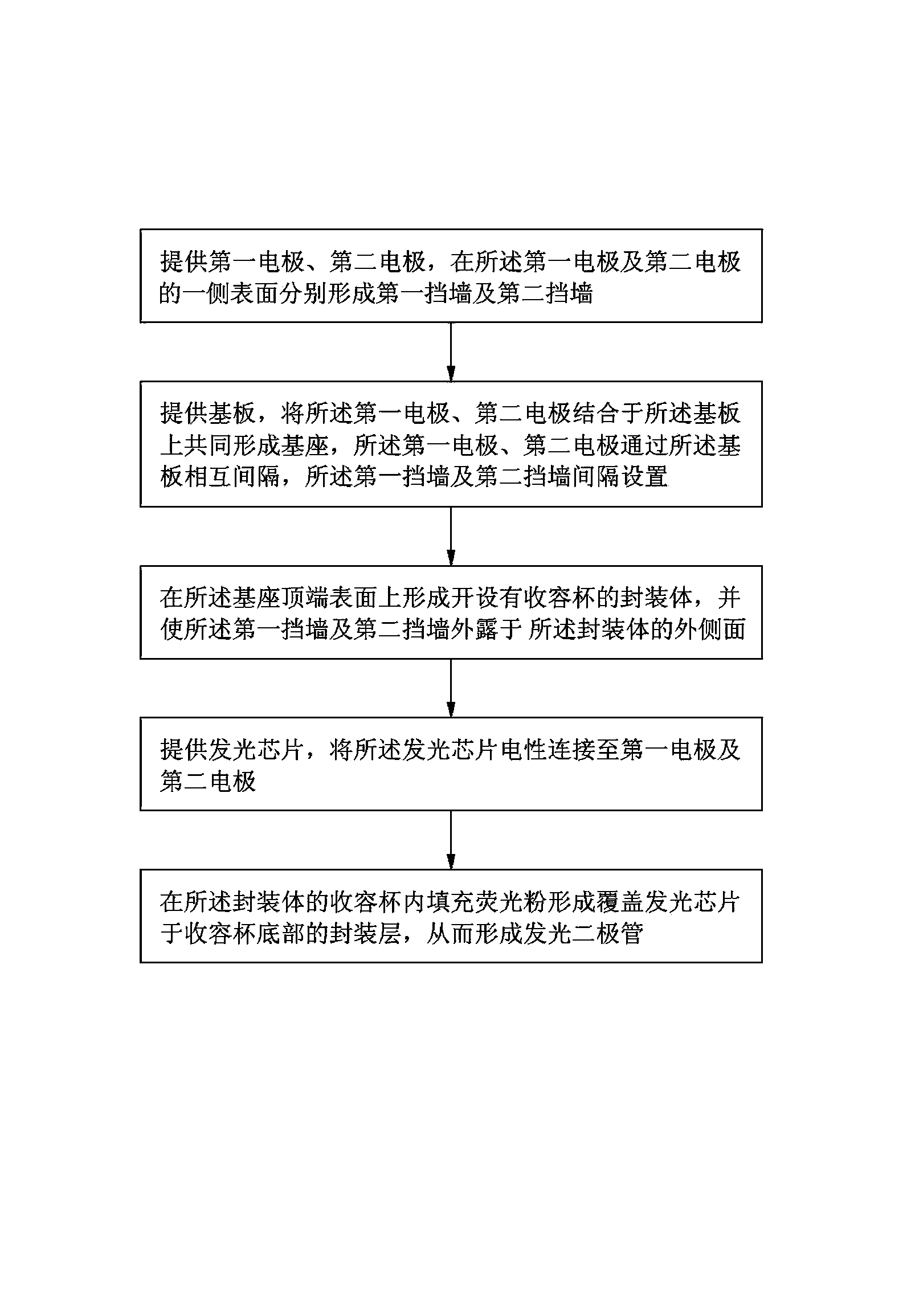
[0020] figure 1 A schematic diagram of the production process of the light-emitting diode provided by the present invention is shown, which includes:

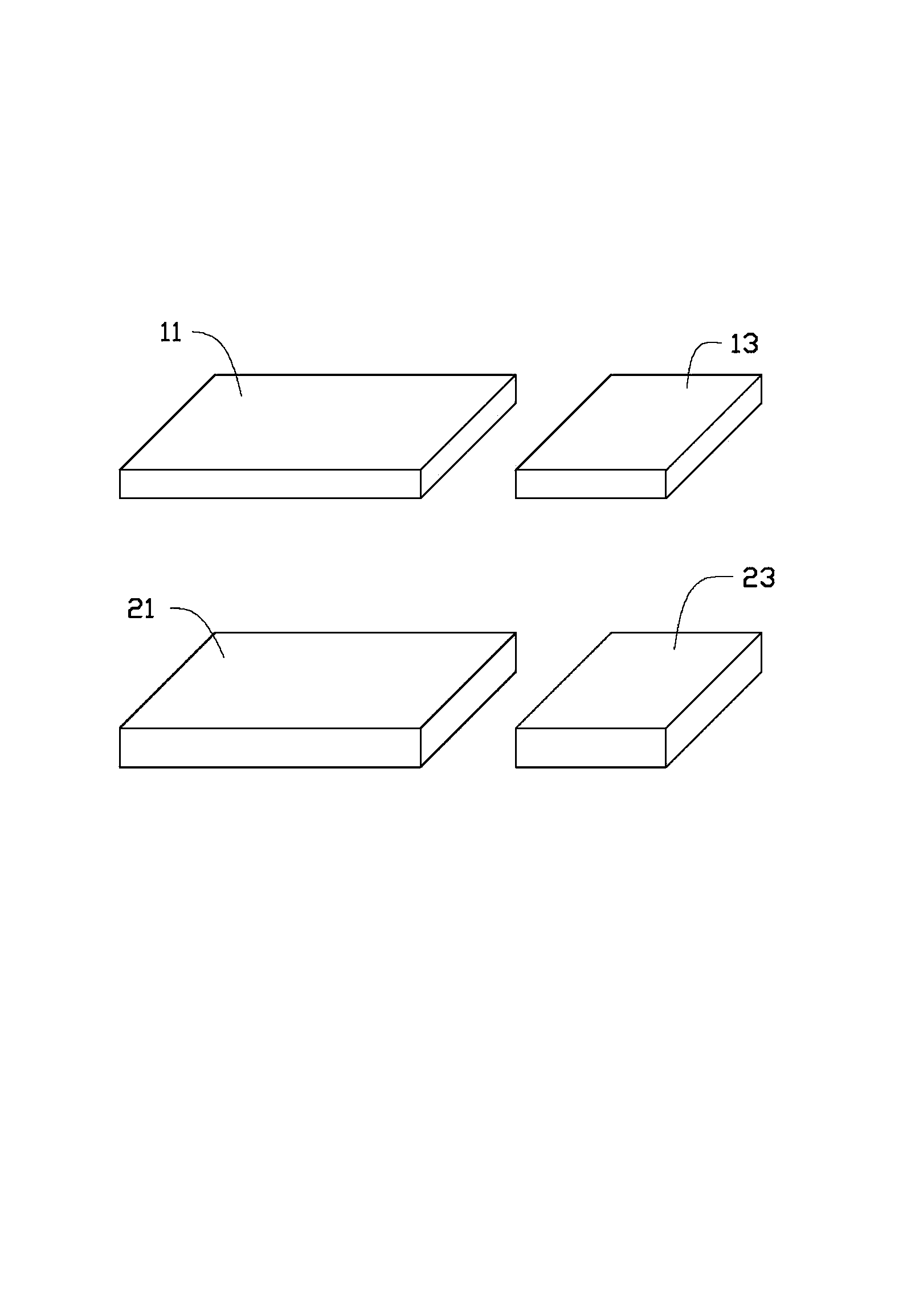
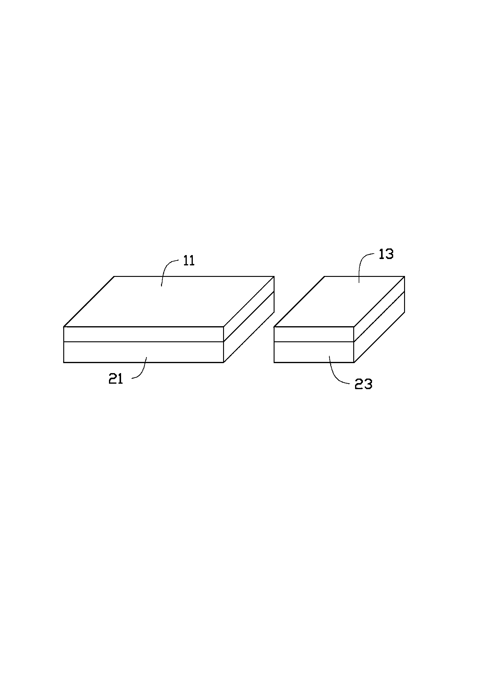
[0021] A first electrode 11 and a second electrode 13 are provided, and a first barrier wall 15 and a second barrier wall 17 are respectively formed on one side surface of the first electrode 11 and the second electrode 13;

[0022] A substrate 30 is provided, the first electrode 11 and the second electrode 13 are combined on the substrate 30 to form a base 40, the first electrode 11 and the second electrode 13 are separated from each other by the substrate 30, and the first electrode 11 and the second electrode 13 are separated from each other by the substrate 30. A retaining wall 15 and a second retaining wall 17 are arranged at intervals;

[0023] A package body 50 with a receiving cup 51 is formed on the top surface of the base 40, and the first retaining wall 15 and the second retaining wall 17 are exposed on the outer su...


PUM


Abstract

A method for manufacturing a light emitting diode comprises the following steps that a first electrode and a second electrode are provided, the surface of one side of the first electrode and the surface of one side of the second electrode are provided with a first retaining wall and a second retaining wall respectively; a substrate is provided, the first electrode and the second electrode are combined to the substrate to form a base, the first electrode is separated from the second electrode through the substrate, and the first retaining wall and the second retaining wall are arranged at intervals; a capsule provided with a containing cup is arranged on the surface of the top end of the base, and the first retaining wall and the second retaining wall are exposed out of the outer side face of the capsule; a light-emitting chip is provided and is electrically connected to the first electrode and the second electrode; the containing cup of the capsule is filled with fluorescent powder to form a capsulation layer for covering the light-emitting chip to the bottom of the containing cup, and accordingly the light emitting diode is formed.

Description

technical field [0001] The invention relates to a semiconductor manufacturing method, in particular to a light emitting diode manufacturing method. Background technique [0002] As a new light source, light-emitting diodes have been widely used in various lighting occasions, and have a tendency to replace traditional light sources. [0003] The existing manufacturing method of light-emitting diodes generally includes providing a substrate, forming two electrodes on the substrate, then forming a light-emitting chip electrically connected to the electrodes on the electrodes, and then forming a light-emitting chip covering the electrodes and the light-emitting chip on the substrate. package, thereby forming a light emitting diode. However, for the light-emitting diode made by this method, because its two electrodes are arranged on the bottom of the package and only its bottom surface is exposed, when this light-emitting diode is installed, generally only the bottom surface of ...

Claims


Application Information

Patent Timeline
IPC IPC(8): H01L33/00
Inventor 林新强陈滨全
Owner 广东艾力森数码电器有限公司
Features
  • R&D
  • Intellectual Property
  • Life Sciences
  • Materials
  • Tech Scout
  • Unparalleled Data Quality
  • Higher Quality Content
  • 60% Fewer Hallucinations
Learn More