Printed circuit board, manufacturing method thereof and electronic device

A technology for printed circuit boards and manufacturing methods, applied in printed circuit parts, structural connection of printed circuits, multi-layer circuit manufacturing, etc., can solve problems such as poor drop resistance and lack of elasticity in the PCB area, and achieve strong drop resistance , to achieve the effect of sticking devices on both sides and facilitating the shape

Active Publication Date: 2013-12-04
LENOVO (BEIJING) LTD
View PDF2 Cites 2 Cited by
  • Summary
  • Abstract
  • Description
  • Claims
  • Application Information

AI Technical Summary

Problems solved by technology

However, the two PCB areas still have planar restrictions on the structural design, the PCB area is still strong and lacks elasticity, and the drop resistance is poor

Method used


Image

  • Printed circuit board, manufacturing method thereof and electronic device
  • Printed circuit board, manufacturing method thereof and electronic device
  • Printed circuit board, manufacturing method thereof and electronic device

Examples


Embodiment Construction

[0034] The main realization principles, specific implementation modes and corresponding beneficial effects of the technical solutions of the embodiments of the present invention will be described in detail below in conjunction with each accompanying drawing.

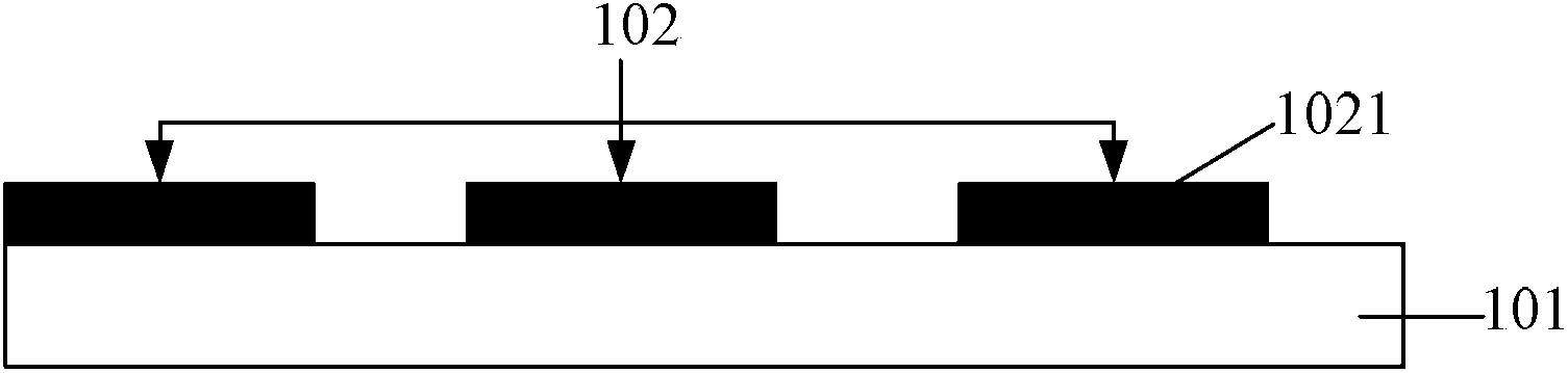
[0035] In order to solve the problems existing in the prior art, the embodiment of the present invention provides a printed circuit board, such as figure 1 shown, including:

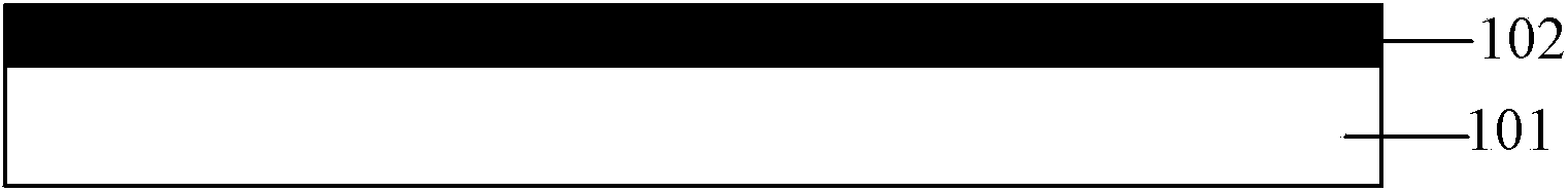
[0036] The first circuit board 101 whose etched flexibility parameter is the first parameter and the second circuit board 102 whose etched flexibility parameter is the second parameter, the first parameter is greater than the second parameter;

[0037] Wherein, the etched first circuit board 101 is connected to the etched second circuit board 102 .

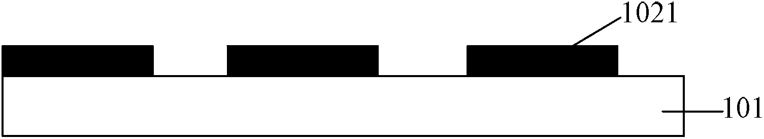
[0038] When the etched second circuit board 102 includes at least two independent second circuit sub-boards 1021, at least two of the independent second circuit sub-boards 1021 pass through at least a...


PUM


Abstract

The invention relates to the technical field of communication, in particular to a printed circuit board and a manufacturing method thereof. The printed circuit board comprises a first circuit board enabling a flexibility parameter after etching to serve as a first parameter and a second circuit board enabling a flexibility parameter after etching to serve as a second parameter. The manufacturing method comprises the steps of respectively performing etching on the first circuit board and the second circuit board according to a preset circuit pattern; and enabling the etched first circuit board to be connected with the etched second circuit board. According to the printed circuit board, the manufacturing method of the printed circuit board and an electronic device, the first circuit board and the second circuit board are respectively cut into corresponding shapes according to the preset circuit pattern after undergoing press fit, and the cut first circuit board and the cut second circuit board are connected. Due to the fact that the formed circuit board has a certain elasticity, the anti-breaking capability is high; besides, the formed circuit board can be bent randomly, and diversification of electronic product forms is facilitated. In addition, the cost of the formed circuit board is lower than that of the first circuit board, and device adhesion to two sides can be achieved.

Description

technical field [0001] The invention relates to the technology in the communication field, in particular to a printed circuit board, a manufacturing method thereof, and an electronic device. Background technique [0002] At present, the material of most PCB (Printed Circuit Board, printed circuit board) boards is hard and the shape is fixed. However, its drop resistance is poor, so due to the lack of elasticity, the components soldered on the PCB may be desoldered due to falling. Moreover, it has planar restrictions on the structural design of the system. For example, the external interfaces soldered on the PCB board must be based on the PCB. [0003] In order to make the PCB no longer rigid, a pure FPC (Flexible Printed Circuit board, flexible printed circuit board) design is proposed in the prior art. However, where the device needs to be welded on the FPC, a rigid "reinforcing board" needs to be attached to the FPC on the other side of the device where the device is wel...

Claims


Application Information

Patent Timeline
Patent Type & Authority Applications(China)
IPC IPC(8): H05K1/14H05K3/46
Inventor 张笑为余秀青
Owner LENOVO (BEIJING) LTD
Why Eureka
Try Eureka