
In-cell touch display panel

A touch display panel, embedded technology, applied in the direction of instrument, electrical digital data processing, data processing input/output process, etc., to meet the requirements of narrow frame design and reduce the area.

Inactive Publication Date: 2014-01-01
AU OPTRONICS CORP
View PDF3 Cites 30 Cited by
  • Summary
  • Abstract
  • Description
  • Claims
  • Application Information

AI Technical Summary

Problems solved by technology

The array of active components is arranged in the display area

Method used


Image

  • In-cell touch display panel
  • In-cell touch display panel
  • In-cell touch display panel

Examples


Embodiment Construction

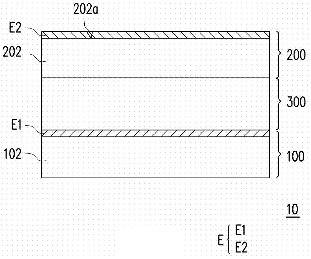
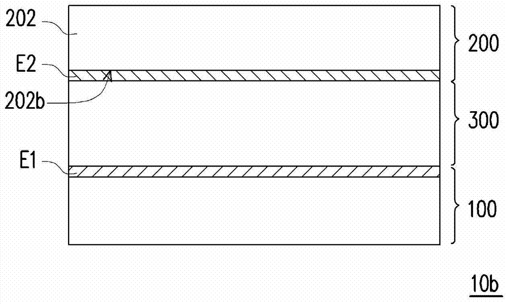
[0055] Figure 1A It is a schematic cross-sectional view of an in-cell touch display panel according to an embodiment of the present invention. Please refer to Figure 1A The in-cell touch display panel 10 includes an active element array substrate 100 , an opposite substrate 200 and a display medium layer 300 . The opposite substrate 200 is disposed corresponding to the active array substrate 100 , wherein the display medium layer 300 is sandwiched between the active device array substrate 100 and the opposite substrate 200 .

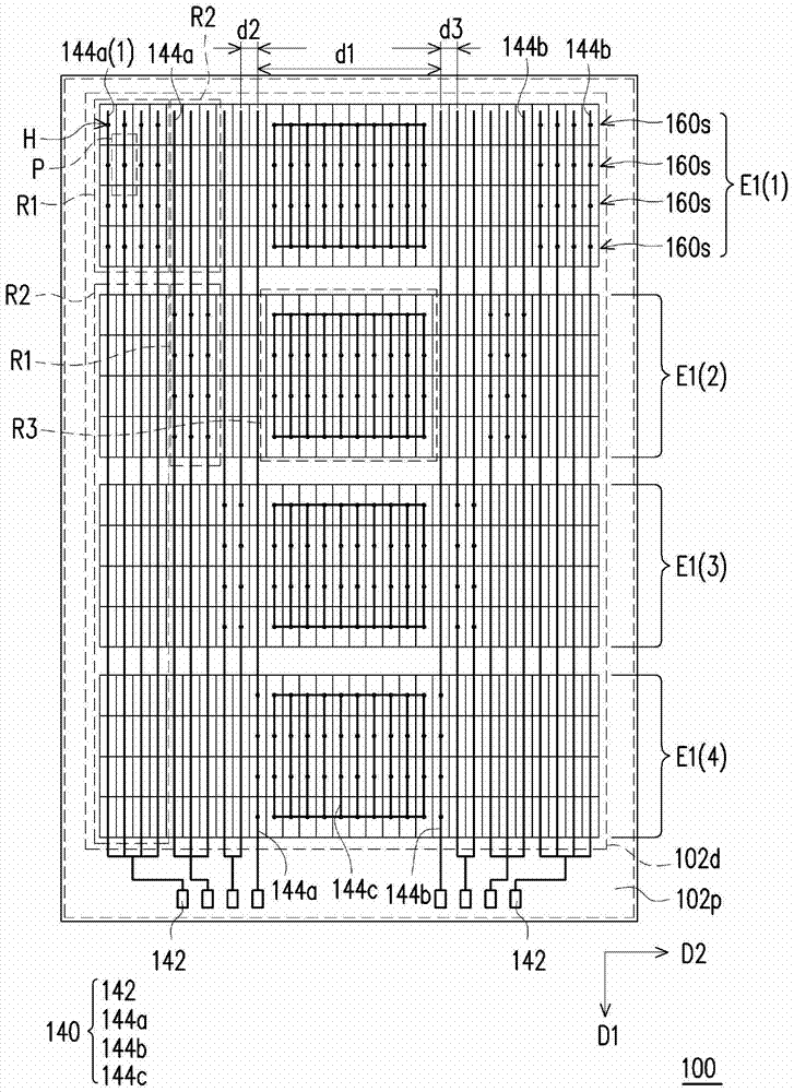
[0056] figure 2 It is a schematic top view of the active device array substrate 100 . Please refer to figure 2 The active device array substrate 100 has a display area 102d and a peripheral area 102p, wherein the peripheral area 102p is disposed around the display area 102d. There are a plurality of sub-pixel units P on the active device array substrate 100, image 3 An enlarged schematic view of one of the sub-pixel units P is shown. Please ref...


PUM


Abstract

The invention provides an in-cell touch display panel comprising an active component array substrate, opposite substrates and a display dielectric layer. The active component array substrate comprises a plurality of active components, a plurality of pixel electrodes, a first insulating layer, a conducting layer, a plurality of second insulating layers and a plurality of common electrodes. The conducting layer comprises a plurality of connection pads and a plurality of first connecting wires. The first connecting wires extend in a first direction, are located in a display area and are connected with the corresponding connection pads. The second insulating layers are disposed on the conducting layer and comprise a plurality of contact windows. The common electrodes are disposed on the second insulating players and are arranged into a plurality of common electrode serials extending in a second direction. More than two common electrode serials are connected to so that first electrode wires with the number of N, which are arranged in order in the second direction, are formed. The Jth first connecting wire is connected to the Kth first electrode wire through the corresponding contact window.

Description

technical field [0001] The present invention relates to a touch display panel, in particular to an embedded touch display panel. Background technique [0002] With the rapid development and application of information technology, wireless mobile communication and information home appliances, many information products have changed from traditional keyboard or mouse input devices to touch control panel as an input device. [0003] Currently, touch panels can be roughly classified into resistive, capacitive, infrared and ultrasonic touch panels, among which resistive touch panels and capacitive touch panels are the most common products. As far as the capacitive touch panel is concerned, the multi-touch feature provides a more user-friendly operation mode, making the capacitive touch panel favored by the market. [0004] Generally speaking, a touch display panel has a display area and a peripheral area, wherein the display area is provided with a sensing array to sense the occu...

Claims


Application Information

Patent Timeline
IPC IPC(8): G06F3/041G06F3/044
Inventor 许哲嘉马玫生翁裕复郑暐柔吕英齐李锡烈
Owner AU OPTRONICS CORP
Features
  • Generate Ideas
  • Intellectual Property
  • Life Sciences
  • Materials
  • Tech Scout
  • Unparalleled Data Quality
  • Higher Quality Content
  • 60% Fewer Hallucinations
Learn More