Grid drive circuit, array substrate and liquid crystal display device

A gate drive circuit and gate signal technology, which is applied in the field of array substrates, liquid crystal display devices, and gate drive circuits, can solve problems such as poor display effects, and achieve the effect of improving display effects

Active Publication Date: 2014-01-08
HEFEI BOE OPTOELECTRONICS TECH +1
View PDF5 Cites 8 Cited by
  • Summary
  • Abstract
  • Description
  • Claims
  • Application Information

AI Technical Summary

Problems solved by technology

[0003] However, the change of the gate voltage will cause the pixel electrode voltage to generate a jump voltage (Feed through Voltage) through the parasitic capacitance or storage capacitance. Therefore, after the pixel TFT is turned off, the process of the gate

Method used


Image

  • Grid drive circuit, array substrate and liquid crystal display device
  • Grid drive circuit, array substrate and liquid crystal display device
  • Grid drive circuit, array substrate and liquid crystal display device

Examples


Example Embodiment

[0038] The technical solutions in the embodiments of the present invention will be clearly and completely described below with reference to the accompanying drawings in the embodiments of the present invention. Obviously, the described embodiments are only a part of the embodiments of the present invention, but not all of the embodiments. Based on the embodiments of the present invention, all other embodiments obtained by those of ordinary skill in the art without creative efforts shall fall within the protection scope of the present invention.
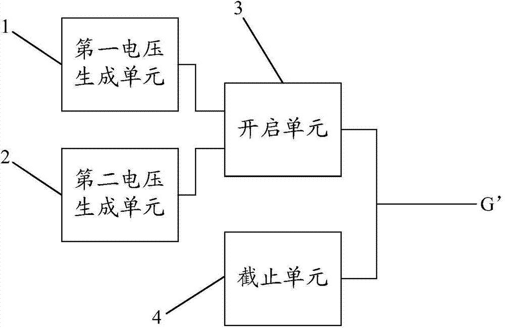
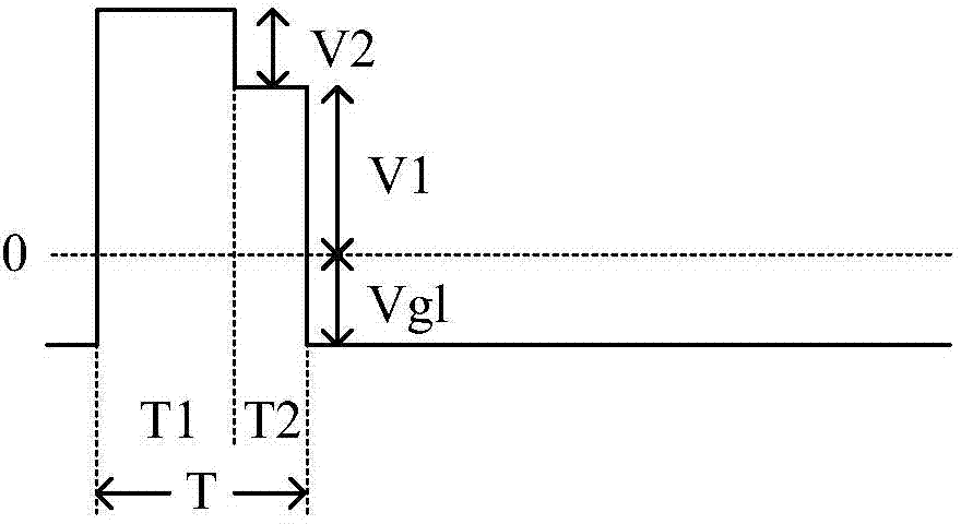
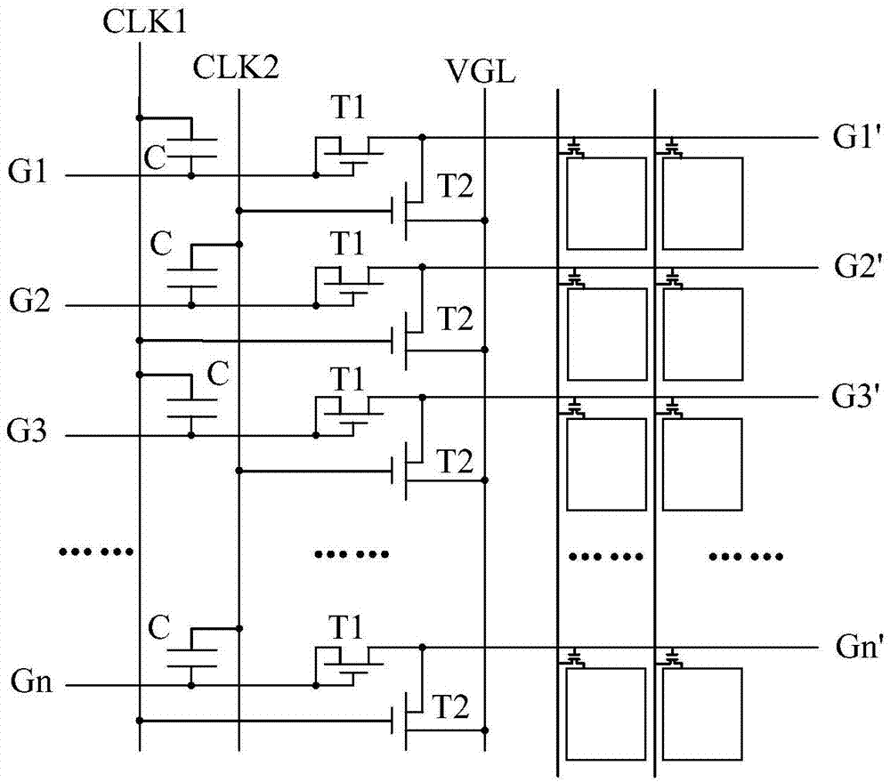
[0039] like figure 1 and figure 2 As shown, an embodiment of the present invention provides a gate driving circuit, including: a first voltage generating unit 1 for generating a first voltage V1 in one line scanning time T, which is sequentially composed of the first stage T1 and the The second stage T2 consists of the second voltage generating unit 2 for generating the second voltage V2 in the first stage T1; the opening unit 3 for...


PUM


Abstract

The invention discloses a grid drive circuit, a method thereof, an array substrate and a liquid crystal display device and relates to the technical field of liquid crystal display, so an actual pixel voltage is closer to a charge voltage and the display effect is improved. The grid drive circuit comprises a first voltage generating unit, a second voltage generating unit, a starting unit and a cut-off unit; the first voltage generating unit is used for generating a first voltage in one-line scanning time, wherein the one-line scanning time is formed by a first stage and a second stage; the second voltage generating unit is used for generating a second voltage in the first stage; the starting unit is used for outputting the sum of the first voltage and the second voltage in the first stage and outputting the first voltage in the second stage; the cut-off unit is used for outputting a cut-off voltage at the end of the one-line scanning time.

Description

technical field [0001] The present invention relates to the technical field of liquid crystal display, in particular to a gate drive circuit, an array substrate and a liquid crystal display device. Background technique [0002] The current liquid crystal display usually controls the thin film transistor (Thin Film Transistor, TFT) of each row of pixels through the second-order gate voltage, that is, provides high voltage and low voltage. When the high voltage is high, the pixel TFT is turned on, and the data line charges the pixel electrode to Pixel voltage, the pixel TFT is turned off when the voltage is low, and the pixel voltage is stored. [0003] However, the change of the gate voltage will cause the pixel electrode voltage to generate a jump voltage (Feed through Voltage) through the parasitic capacitance or storage capacitance. Therefore, after the pixel TFT is turned off, the process of the gate voltage changing from high voltage to low voltage will make The pixel e...

Claims


Application Information

Patent Timeline
IPC IPC(8): G09G3/36
Inventor 刘荣铖
Owner HEFEI BOE OPTOELECTRONICS TECH
Why Eureka
Try Eureka