

Single-substrate display panel and manufacturing method thereof
A technology for a display panel and a manufacturing method, which is applied in optics, instruments, nonlinear optics, etc., can solve the problems of large weight and thickness of liquid crystal display panels, which cannot meet the requirements of liquid crystal displays, and achieves the improvement of display effect and the reduction of weight and thickness. Effect
- Summary
- Abstract
- Description
- Claims
- Application Information
AI Technical Summary
Problems solved by technology
Method used
Image

Examples
Embodiment 1
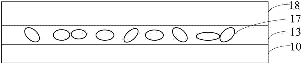
[0054] figure 1 Shown is a schematic structural diagram of a single-substrate display panel according to Embodiment 1 of the present invention. Such as figure 1 As shown, the stand-alone panel display panel provided by the present invention includes a parallel electric field substrate 10. The parallel electric field substrate 10 can be an array substrate of parallel electric field modes such as IPS, FFS, and ADS commonly used in the display field, or can be other simple passive parallel substrates. Electric field, such as pen segment type, passive matrix type, etc.; the display medium layer 13 formed above the parallel electric field substrate 10, wherein the display medium layer 13 includes liquid crystal molecules and a matrix, wherein the matrix wraps the liquid crystal molecules to form a liquid crystal group 17, and the liquid crystal The specific shape of the group is spherical or other shapes. Normal refractive index n of liquid crystal molecules o and the refractive...
Embodiment 2
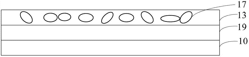
[0062] figure 2 Shown is a schematic structural diagram of a single-substrate display panel in Embodiment 2 of the present invention, as shown in figure 2 As shown, the single substrate structure of the present invention includes a parallel electric field substrate 10, and a display medium layer 13 formed above the parallel electric field substrate 10. The display medium layer 13 includes liquid crystal molecules and a matrix, wherein the matrix wraps the liquid crystal molecules to form a liquid crystal group 17. The above-mentioned structure can be specifically the same as the first embodiment. Compared with Embodiment 1, the parallel electric field substrate 10 in this embodiment is provided with a color filter layer 19 , and the color filter layer 19 is formed above the display medium layer 13 .
[0063] In this embodiment, the matrix constituting the display medium layer 13 includes a liquid crystal polymer with a rigid structure. Liquid crystal polymers with a rigid...
Embodiment 3
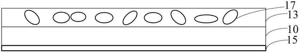
[0068] image 3 Shown is a schematic structural diagram of a single-substrate display panel according to Embodiment 3 of the present invention. Such as image 3 As shown, the stand-alone panel display panel provided by the present invention includes a parallel electric field substrate 10. The parallel electric field substrate 10 can be an array substrate of parallel electric field modes such as IPS, FFS, and ADS commonly used in the display field, or can be other simple passive parallel substrates. Electric field, such as pen segment type, passive matrix type, etc.; the display medium layer 13 formed above the parallel electric field substrate 10, wherein the display medium layer 13 includes liquid crystal molecules and a matrix, wherein the matrix wraps the liquid crystal molecules to form a liquid crystal group 17, and the liquid crystal The specific shape of the group is spherical or other shapes. A lower polarizer 15 is also attached below the substrate 10 . The matrix ...
PUM
 Abstract
Description
Claims
Application Information