Photosensitive film, method for producing capacitance type input device, capacitance type input device, and image display apparatus using the same

a capacitance type input and capacitance type technology, applied in the direction of photomechanical equipment, instruments, pulse techniques, etc., can solve the problems of difficult to provide white decorative layers that satisfy the aforementioned characteristics. , to achieve the effect of high yield, good brightness, whiteness, adhesion and adhesion

Active Publication Date: 2014-12-25
FUJIFILM CORP
View PDF4 Cites 17 Cited by
  • Summary
  • Abstract
  • Description
  • Claims
  • Application Information

AI Technical Summary

Benefits of technology

[0043]According to the invention, there may be provided a photosensitive film that is capable of providing a white decorative layer tha

Problems solved by technology

As a result of investigations by the present inventors, it has been found that in the case where a white decorative layer is formed by the methods described in the literatures, it is impossible to provide ones that satisfy all the characteristics includin

Method used


Image

  • Photosensitive film, method for producing capacitance type input device, capacitance type input device, and image display apparatus using the same
  • Photosensitive film, method for producing capacitance type input device, capacitance type input device, and image display apparatus using the same
  • Photosensitive film, method for producing capacitance type input device, capacitance type input device, and image display apparatus using the same

Examples


example 1

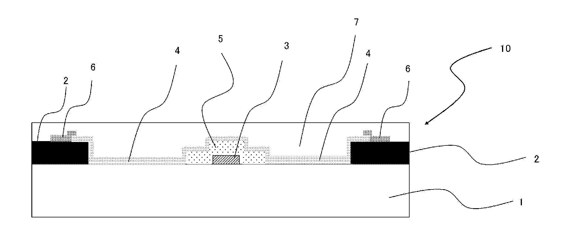
[0227]Preparation of Photosensitive Film of Invention Preparation of Photosensitive Film of Example 1, as Photosensitive Film L1 for forming Decorative Layer

[0228]On a polyethylene terephthalate film having a thickness of 75 μm as a provisional support, a coating liquid for a thermoplastic resin layer having the following formulation H1 was coated with a slit nozzle and dried. A coating liquid for an intermediate layer having the following formulation P1 was then coated and dried. A coating liquid for a white photocurable resin layer having the following formulation L1 was then further coated and dried. Thus, a thermoplastic resin layer having a dry thickness of 15.1 μm, an intermediate layer having a dry thickness of 1.6 μm and a white photocurable resin layer having a dry thickness of 35 μm were provided on the provisional support, and finally a protective film (a polypropylene film having a thickness of 12 μm) was adhered under pressure thereon. A transfer material having the pro...

example 2

Production of Photosensitive Film C1 Having Conductive Photocurable Resin Layer Laminated Thereon

[0292]A photosensitive film C1 having a conductive photocurable resin layer laminated thereon was obtained in the same manner as in the preparation of the photosensitive film L1 for forming a decorative layer except that the coating liquid for a white photocurable resin layer in the preparation of the photosensitive film L1 for forming a decorative layer was changed to a coating liquid for forming a conductive photocurable resin layer having the following formulation C1 (the thickness of the conductive photocurable resin layer was 2.0 μm).

Preparation of Coating Liquid for Forming Conductive

Photocurable Resin Layer

Preparation of Silver Nanowire Dispersion (1)

[0293]0.51 g of silver nitride powder was dissolved in 50 mL of pure water to prepare a silver nitride solution. Thereafter, 1N aqueous ammonia was added to the silver nitride solution until the solution became transparent, and pure w...

examples 3 and 4

[0308]Photosensitive films for forming a decorative layer of Examples 3 and 4 were produced in the same manner as in Example 1 except that the formulations L3 and L4 were used instead of the formulation L1 of the coating liquid for a white photocurable resin layer in Example 1, and the monomer / binder ratio was changed to those shown in Table 1. Front plates having formed thereon a decorative layer were formed in the same manner as in Example 1 except that the photosensitive films for forming a decorative layer of Examples 3 and 4 thus produced, and evaluated. The evaluation results are shown in Table 1. Thereafter, front plates 3 and 4, which were capacitance type input devices of Examples 3 and 4, having the decorative layer, the mask layer, the first transparent electrode patterns, the insulating layer pattern, the second transparent electrode patterns, the conductive element other than the first and second transparent electrode patterns, and the transparent protective layer were ...


PUM

PropertyMeasurementUnit
Lengthaaaaaaaaaa
Percent by massaaaaaaaaaa
Electrical conductoraaaaaaaaaa

Abstract

A photosensitive film having a provisional support and a photocurable resin layer, wherein the photocurable resin layer contains a white inorganic pigment, a monomer, a binder and a photopolymerization initiator, the photocurable resin layer has a thickness of from 1 to 40 μm, and the photocurable resin layer has a content of the white inorganic pigment of from 30 to 50% by mass is capable of providing a white decorative layer that is good in brightness, whiteness, reticulation, adhesion, development residue and unevenness, in a high yield.

Description

CROSS-REFERENCE TO RELATED APPLICATIONS[0001]This application is a continuation application of International Application No. PCT / JP2013 / 056736, filed Mar. 12, 2013, which in turn claims the benefit of priority from Japanese Application No. 2012-058243, filed Mar. 15, 2012, the disclosures of which Applications are incorporated by reference herein in their entirety.BACKGROUND OF THE INVENTION[0002]1. Field of the Invention[0003]The present invention relates to a decorative photosensitive film for producing a capacitance type input device capable of detecting a touch position of a finger as a change of capacitance, a method for producing a capacitance type input device, a capacitance type input device obtained by the production method, and an image display apparatus equipped with the capacitance type input device as a constitutional component.[0004]2. Background Art[0005]In recent years, electronic equipments, such as mobile telephones, car navigation systems, personal computers, tick...

Claims


Application Information

Patent Timeline
IPC IPC(8): G06F3/044H03K17/96H01H11/06G06F1/16
CPCG06F3/044G06F1/1643H03K2017/9613H01H11/06H03K2217/960755H03K17/9622G03F7/027G03F7/105Y10T29/49105Y10T428/264G06F3/0446C09K2323/05G06F3/0443G06F2203/04111G03F7/0047G03F7/028G03F7/032G06F3/041G06F3/0445G03F7/004G03F7/00G03F7/42G03F7/322G03F7/11
Inventor GOTOH, HIDENORIYOSHINARI, SHINICHI
Owner FUJIFILM CORP
Why Eureka
Try Eureka