Touch display panel

a touch display panel and display panel technology, applied in the field of touch display panels, can solve the problems of unstable display images, limited display pixels resolution, user portability burden, etc., and achieve the effect of reducing the thickness and weight of the touch display panel

Active Publication Date: 2016-01-21
ILI TECHNOLOGY CORPORATION
View PDF5 Cites 19 Cited by
  • Summary
  • Abstract
  • Description
  • Claims
  • Application Information

AI Technical Summary

Benefits of technology

[0006]It is a primary object of the present invention to provide a touch display panel. Without interfering with functions of a display panel, the...

Problems solved by technology

The overall thickness and weight of the panels are greater than those of one single display panel, resulting in a burden in user portability.
Further, as the touch sensing circuit needs metal conducting lines in different directions ...

Method used


Image

  • Touch display panel
  • Touch display panel
  • Touch display panel

Examples


fifth embodiment

[0039]In the embodiment, the touch display panel 600 is an IPS display panel. Thus, a color filter substrate 614 does not include a common electrode layer, and the array substrate 604 may further include a common electrode pattern 616 disposed between the first substrate 112 and the liquid crystal layer 138. In the embodiment, the second substrate 140, the black matrix layer 142, the color filter layer 144, the protection layer 146, the common electrode pattern 616 and the pixel electrodes 612 are identical to those in the fifth embodiment, and the associated description shall be omitted herein. In another embodiment, the touch display panel may be a TN display panel. That is, the color filter substrate includes a common electrode layer, the array substrate does not include a common electrode pattern, and the pixel electrodes do not include gaps.

first embodiment

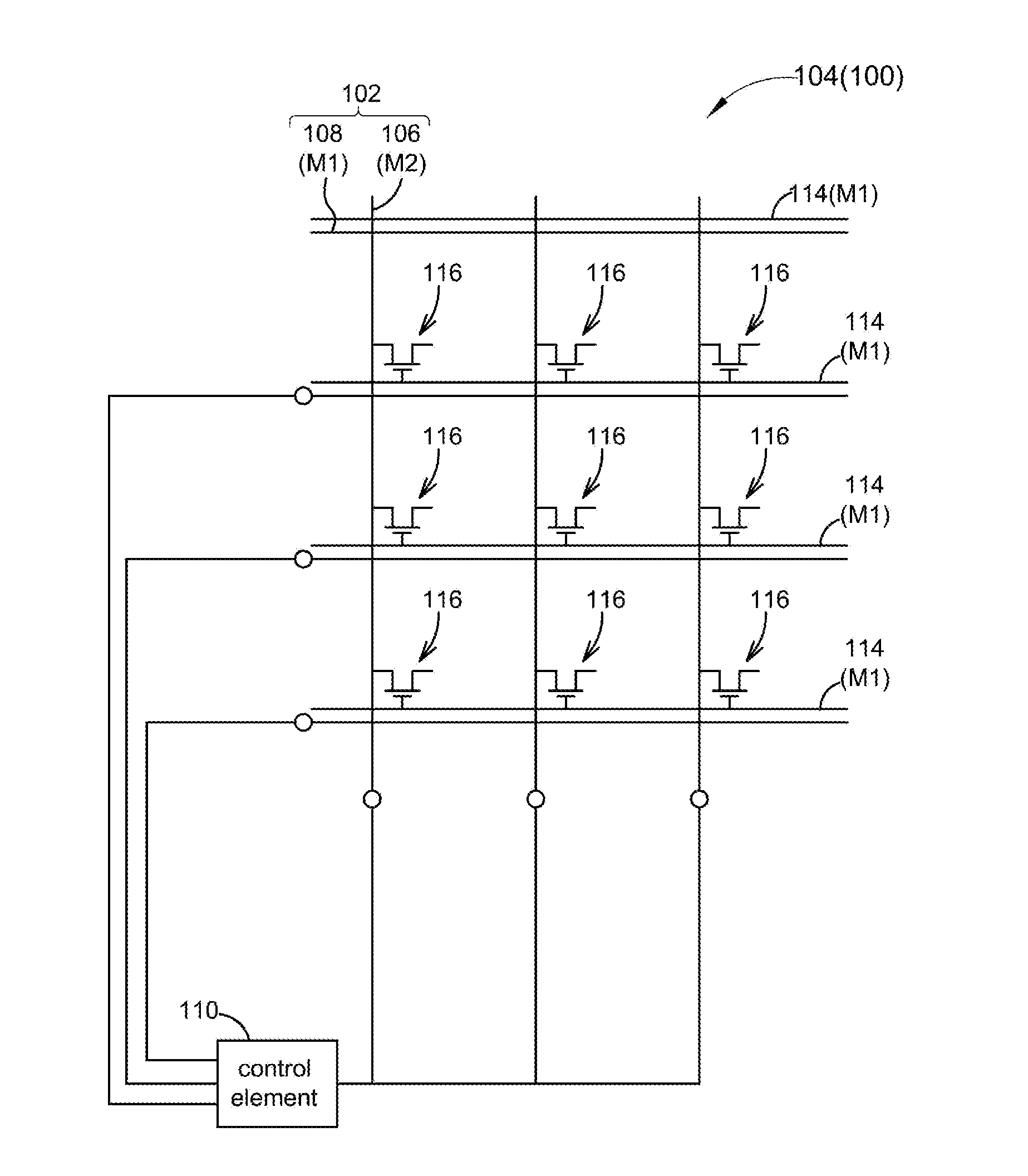
[0040]Details of how the touch display panel of the embodiment simultaneously provides image display and touch sensing functions are given below. Referring to FIG. 4, compared to the first embodiment, the sensing signals Rx of the embodiment are sensed by the gate lines 114. The gate lines 114 transmit at least one of the pixel switch signals G1 to Gn in the display period DT, and transmit the sensing signals Rx instead of the pixel switch signals G1 to Gn in the touch control period TT. More specifically, in the display period DT, the switching elements 610 switch and electrically connect the gate lines 114 to the first conducting lines 606. Thus, the control element 110 transmit the pixel switch signals G1 to Gn to the gate lines 114 via the first conducting lines 606, and transmit the pixel voltage signals F to the data lines 106. In the touch control period TT, the control element 110 transmits the touch driving signals T to the data lines 106, and the switching elements 610 swi...


PUM


Abstract

A touch display panel includes a substrate, a plurality of data lines, a plurality of touch sensing lines, and a plurality of gate lines. The data lines are disposed above the substrate, and extend along a first direction. The touch sensing lines are disposed above the substrate, extend along a second direction different from the first direction, and intersect with the data lines. The gate lines are disposed above the substrate, extend along the second direction, and intersect with the data lines. The touch sensing lines or the gate lines and the data lines form touch sensing elements.

Description

[0001]This application claims the benefit of U.S. Provisional Application Ser. No. 62 / 027,236, filed Jul. 21, 2014, the subject matter of which is incorporated herein by reference.BACKGROUND OF THE INVENTION[0002]1. Field of the Invention[0003]The invention relates in general to a touch display panel, and more particularly, to a touch display panel in which a touch sensing element is formed by a touch sensing line or a gate line and a data line.[0004]2. Description of the Related Art[0005]A conventional touch display panel is formed by directly adhering a touch panel with a display panel. The overall thickness and weight of the panels are greater than those of one single display panel, resulting in a burden in user portability. There are currently display panels integrated with the touch control function. However, an additional touch sensing circuit is an independent unit outside a driving circuit of the display panel. Further, as the touch sensing circuit needs metal conducting lin...

Claims


Application Information

Patent Timeline
IPC IPC(8): G09G3/36G02F1/1333G06F3/041G06F3/044
CPCG09G3/3648G06F3/0416G06F3/044G06F3/0412G09G2310/0202G06F2203/04107G06F2203/04105G09G2310/08G02F1/13338G06F3/04164G06F3/04166G06F3/0443G06F3/0448G06F2203/04101G06F2203/04103G06F2203/04111G09G3/3614G09G2300/0408G09G2300/043
Inventor LIU, CHI KANGHUNG, GUO-KIANG
Owner ILI TECHNOLOGY CORPORATION
Why Eureka
Try Eureka