

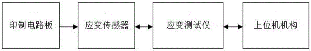
A printed circuit board stress and strain testing system
A technology of stress and strain testing and printed circuit boards, which is applied in the direction of electric/magnetic solid deformation measurement and electromagnetic measurement devices, etc., which can solve the problems of high precision and destructibility of electronic products, which cannot meet the needs of technological development, etc.
- Summary
- Abstract
- Description
- Claims
- Application Information
AI Technical Summary
Problems solved by technology
Method used
Image

Examples
Embodiment Construction
[0019] In order for those skilled in the art to better understand the technical solutions provided by the present invention, the following will be described in conjunction with specific embodiments.
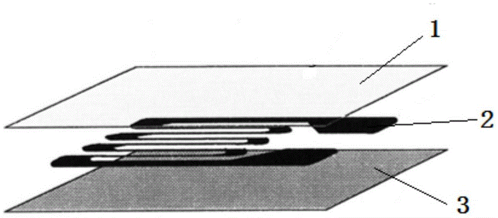
[0020] Stress: When an object is deformed due to external causes (force, temperature change, etc.), an internal force that interacts between various parts of the object is generated to resist the effect of this external cause. This internal force is called stress.
[0021] Strain: It is defined in mechanics as the amount of deformation per unit length produced when a tiny material element is subjected to stress.
[0022] Strain effect: When a conductor or semiconductor material is mechanically deformed under the action of an external force, its resistance value changes accordingly. This phenomenon is called "strain effect".
[0023] Strain electrical measurement method: It is an experimental stress analysis method that uses a resistance strain gauge to measure the surface strain ...
PUM
 Abstract
Description
Claims
Application Information