electronic device

An electronic device and current zero point technology, applied in the direction of circuits, antenna supports/mounting devices, electrical components, etc., can solve the problem of destroying the overall appearance design of electronic devices, and achieve the effect of ensuring radiation efficiency

Active Publication Date: 2016-08-10
ACER INC
View PDF7 Cites 0 Cited by
  • Summary
  • Abstract
  • Description
  • Claims
  • Application Information

AI Technical Summary

Problems solved by technology

However, this design method will destroy the overall appearance design of the electronic device
[0004] In other words, how to balance the production cost of the electronic device and the radiation efficiency of the antenna has become a major challenge in the design of the electronic device in response to the thinning and appearance design requirements of the electronic device.

Method used


Image

  • electronic device
  • electronic device
  • electronic device

Examples


Embodiment Construction

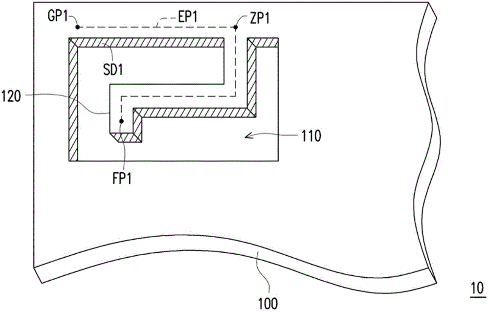
[0027] figure 1 It is a schematic diagram of a partial structure of an electronic device according to an embodiment of the present invention. Please refer to figure 1 , the electronic device 10 includes a metal shell 100 , a first opening 110 , a first metal wiring 120 , a first ground point GP 1 , a first zero current point ZP1 , and a first feeding point FP 1 . Wherein, the first opening 110 runs through the metal casing 100 . The first metal wiring 120 is located in the first opening 110 . In addition, the first end of the first metal wiring 120 is electrically connected to the side SD1 of the first opening 110 , and the second end of the first metal wiring 120 has a first feeding point FP1 . In this embodiment, the metal case 100 can be, for example, the back cover of the electronic device 10 , and the first metal wiring 120 is integrally formed with the metal case 100 , but the present invention is not limited to the above-mentioned embodiment.

[0028] The first grou...


PUM


Abstract

The invention provides an electronic device, which includes a metal casing, a first opening, a first metal wiring, a first grounding point and a first current zero point. The first opening runs through the metal casing. The first metal wiring is located in the first opening, and the first end of the first metal wiring is electrically connected to the side of the first opening, and the second end of the first metal wiring has a first feeding point. The first ground point and the first current zero point are located on the side of the first opening. The metal shell utilizes the first exciting path from the first feeding point to the first grounding point to form a first loop antenna to receive or transmit a first radio frequency signal.

Description

technical field [0001] The present invention relates to an electronic device, and more particularly to an electronic device with a loop antenna. Background technique [0002] Due to the progress and development of the times, current electronic devices such as Smart Phones, Tablet PCs, and Notebook PCs are all developing towards thinner and thinner appearances. In addition, in order to attract the attention of consumers, most of the current electronic devices use metal back covers to highlight the uniqueness and appearance of the products. [0003] Generally speaking, in order to meet the thin design requirements, existing electronic devices can use Laser Direct Structuring (LDS) technology to directly form the antenna on the outer surface of the plastic casing by laser, and thereby strive for the antenna. effective radiation space. However, such a design usually requires a relatively high production cost. Furthermore, due to the metallic appearance design, an additional a...

Claims


Application Information

Patent Timeline
Patent Type & Authority Patents(China)
IPC IPC(8): H01Q1/22H01Q1/36H01Q7/00
Inventor 林敬基
Owner ACER INC
Why Eureka
Try Eureka