An addressable electrical modulation imaging spectrum infrared detection chip

An infrared detection and imaging technology, which is applied in measuring devices, optical radiometry, radiation pyrometry, etc., can solve the problems of imaging spectrum modulation and lack of imaging detection capabilities, and achieve high measurement accuracy, flexible spectral imaging methods, and easy to use convenient effect

Active Publication Date: 2015-11-11
HUAZHONG UNIV OF SCI & TECH
View PDF7 Cites 0 Cited by
  • Summary
  • Abstract
  • Description
  • Claims
  • Application Information

AI Technical Summary

Problems solved by technology

However, there is still a lack of imaging detection capabilities such as spatial spectrum parallelism, that is, the imaging spectrum cannot be modulated with the imaging space

Method used


Image

  • An addressable electrical modulation imaging spectrum infrared detection chip
  • An addressable electrical modulation imaging spectrum infrared detection chip

Examples


Embodiment Construction

[0024] In order to make the object, technical solution and advantages of the present invention clearer, the present invention will be further described in detail below in conjunction with the accompanying drawings and embodiments. It should be understood that the specific embodiments described here are only used to explain the present invention, not to limit the present invention. In addition, the technical features involved in the various embodiments of the present invention described below can be combined with each other as long as they do not constitute a conflict with each other.

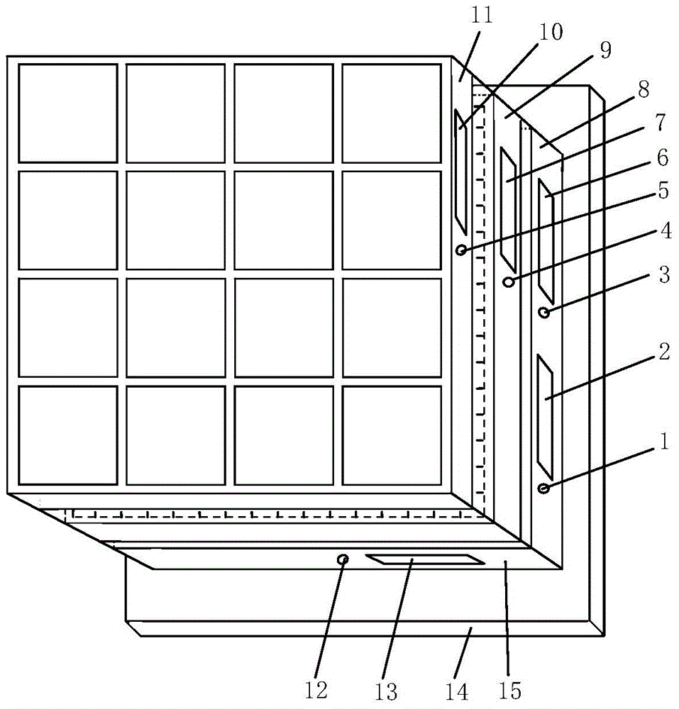
[0025] Such as figure 1 As shown, the addressable electrical modulation imaging spectral infrared detection chip of the embodiment of the present invention includes: a ceramic housing 15 , a metal support cooling plate 14 and an addressable electrical modulation imaging spectral infrared detection structure.

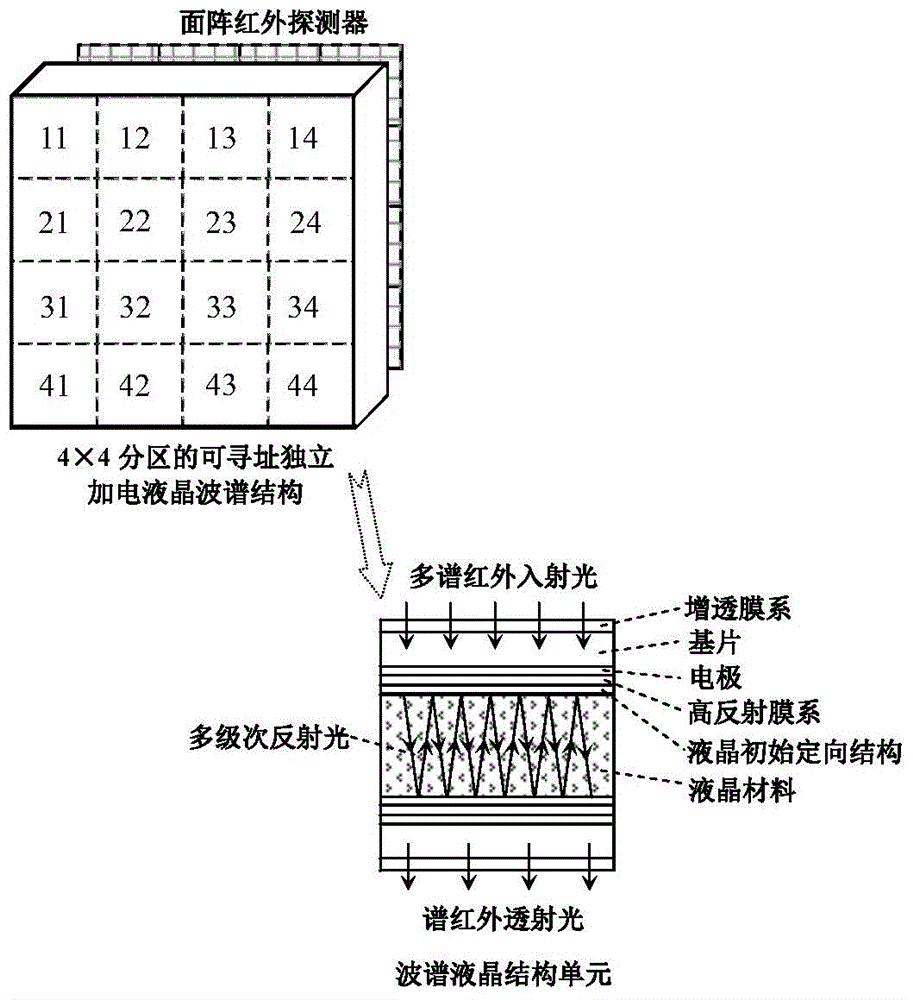
[0026] The addressable electro-tunable imaging spectral infrared detection architectu...


PUM


Abstract

The invention discloses an addressable electrical-modulation imaging-spectrum infrared detection chip which comprises an electrical-modulation imaging-spectrum liquid crystal module, an area-array uncooled infrared detector and a displacement control preprocessing module. The electrical-modulation imaging-spectrum liquid crystal module comprises a plurality of electrical-modulation imaging-spectral liquid crystal structural units, voltage signals and wavelengths, the electrical-modulation imaging-spectrum liquid crystal module is in array distribution and used for allowing a target wave beam to generate multistage second-highest reflection interference, the voltage signals are uploaded in the electrical-modulation imaging-spectral liquid crystal structural units by independent adjustment, and the wavelengths are used for modulating spectrum infrared lightwaves penetrating the electrical-modulation imaging-spectral liquid crystal structural units; the area-array uncooled infrared detector is used for converting spectrum infrared lightwaves penetrating the electrical-modulation imaging-spectrum liquid crystal module into electrical signals; the displacement control preprocessing module is used for subjecting the photoelectric signals to quantization, rectification and non-uniformity correction to obtain target infrared image data. By the infrared detection chip, adjustable rapid spectrum registration, spectrum search, spectrum gaze, spectrum tracking or spectrum lock can be realized; the chip is easy to couple with optical, photoelectrical and mechanical structures and good in environmental adaption.

Description

technical field [0001] The invention belongs to the technical field of infrared imaging detection, and more specifically relates to an addressable electrically adjustable imaging spectrum infrared detection chip. Background technique [0002] Under normal circumstances, the material structure in nature has a markable fingerprint electromagnetic radiation energy spectrum, which is often presented in the form of optical frequency electromagnetic radiation with a nanometer / picometer spectral width. What appears in the field of view of the imaging system is this Targets and scenes with different spectral radiation characteristics. Based on the property of relatively stable spectral radiation characteristics to capture local targets in complex background environments, the targets can be highlighted intuitively through optical hardware, which will effectively reduce the amount of information processing, save electronic resources, and significantly improve the electronic image cons...

Claims


Application Information

Patent Timeline
Patent Type & Authority Patents(China)
IPC IPC(8): G01J5/00
Inventor 张新宇罗俊康胜武佟庆张静李利荣赵慧桑红石谢长生
Owner HUAZHONG UNIV OF SCI & TECH
Why Eureka
Try Eureka