
A test device and test method for high-k metal gate nmos transistors

A test device and metal gate technology, which is applied in the direction of single semiconductor device testing, etc., can solve the problems of long waiting time, deviation of PBTI test results, measurement error, etc., and achieve the effect of easy operation, low cost, and solution to recovery effect

Active Publication Date: 2016-03-30
SEMICON MFG INT (SHANGHAI) CORP
View PDF6 Cites 0 Cited by
  • Summary
  • Abstract
  • Description
  • Claims
  • Application Information

AI Technical Summary

Problems solved by technology

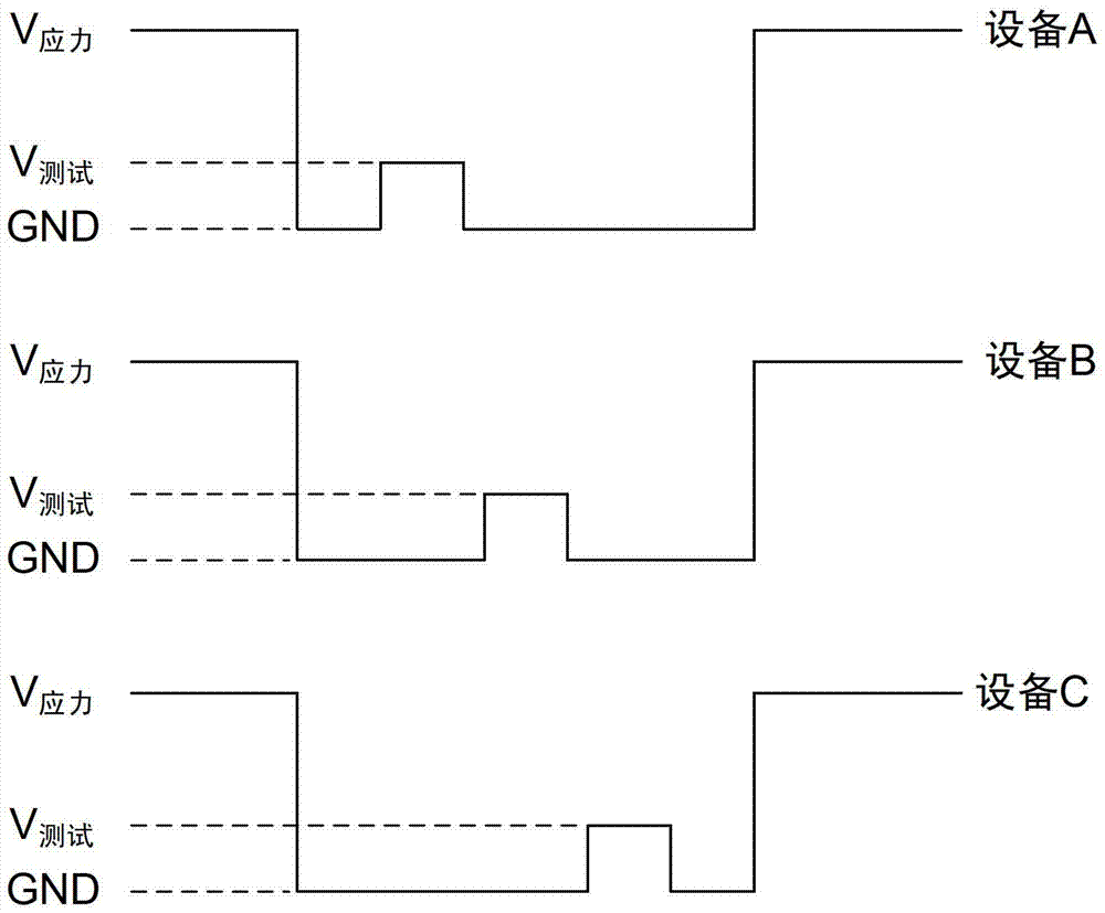
like Figure 1B As shown, since the PLR ​​test is a parallel test system, the waiting time (V 栅极 =GND) is longer, so it is difficult to avoid recovery effects
[0004] This recovery effect will lead to deviations in the test results of PBTI, resulting in measurement errors. Therefore, there is an urgent need for a test device and test method for NMOS transistors to solve the above problems

Method used


Image

  • A test device and test method for high-k metal gate nmos transistors
  • A test device and test method for high-k metal gate nmos transistors
  • A test device and test method for high-k metal gate nmos transistors

Examples


Embodiment Construction

[0024] Next, the present invention will be described more fully with reference to the accompanying drawings, in which embodiments of the invention are shown. However, this invention may be embodied in different forms and should not be construed as limited to the embodiments set forth herein. Rather, these embodiments are provided so that this disclosure will be thorough and complete, and will fully convey the scope of the invention to those skilled in the art. In the drawings, the size and relative sizes of layers and regions may be exaggerated for clarity. Like reference numerals refer to like elements throughout.

[0025] It will be understood that when an element or layer is referred to as being "on," "adjacent," "connected to" or "coupled to" another element or layer, it can be directly on the other element or layer. A layer may be on, adjacent to, connected to, or coupled to other elements or layers, or intervening elements or layers may be present. In contrast, when a...


PUM


Abstract

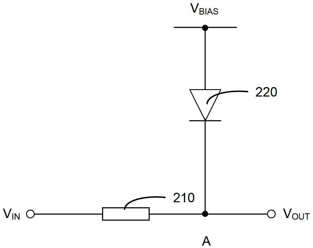
The invention discloses a testing device and a testing method used for an NMOS (n-channel metal oxide semiconductor) transistor in a high-k metal gate. The testing device comprises a resistor and a diode. The resistor is connected between an input end and an output end of the testing device, a positive pole of the diode is used for being connected with a bias voltage source, a negative pole of the diode is connected to the output end of the testing device, the input end of the testing device is used for receiving testing signals, and the output end of the testing device is used for connecting the gate of a to-be-tested NMOS transistor. The testing device is capable of exerting stress upon the to-be-tested NMOS transistor continuously and automatically during the PBTI (positive bias temperature instability) testing process, so that the problem of restoration effect during the PBTI testing process can be effectively solved; besides, the testing device is easy to operate and basically free of additional hardware, thereby being low in cost.

Description

technical field [0001] The invention relates to a semiconductor manufacturing process, in particular to a test device and a test method for a high-k metal gate NMOS transistor. Background technique [0002] In the high-k metal gate (HKMG) process, the positive bias temperature instability (PositiveBiasTemperatureInstability, PBTI) of NMOS transistors is an evaluation item that cannot be ignored. Compared with the traditional polysilicon gate-silicon oxide process, the PBTI effect of NMOS transistors in high-k metal gates becomes more serious. However, it is well known that the PBTI of high-k metal gate NMOS transistors has a strong self-recovery effect (RecoveryEffect ), that is, when the gate bias is less than or equal to zero, the reliability failure caused by PBTI will largely recover by itself. [0003] In the reliability measurement process, in order to consider the PBTI reliability performance of the high-k metal gate NMOS transistor to the greatest extent, it is nece...

Claims


Application Information

Patent Timeline
Patent Type & Authority Patents(China)
IPC IPC(8): G01R31/26
Inventor 冯军宏甘正浩
Owner SEMICON MFG INT (SHANGHAI) CORP
Learn More