
Process compatible decoupling capacitor and manufacturing method

A technology of decoupling capacitors and capacitors, applied in the direction of capacitors, semiconductor/solid-state device manufacturing, electric solid-state devices, etc., can solve the problem that decoupling capacitors cannot completely meet the requirements

Active Publication Date: 2016-05-18
TAIWAN SEMICON MFG CO LTD
View PDF6 Cites 0 Cited by
  • Summary
  • Abstract
  • Description
  • Claims
  • Application Information

AI Technical Summary

Problems solved by technology

Decoupling capacitors on a particular SOC have not been adequate so far and may create more and more problems in the future

Method used


Image

  • Process compatible decoupling capacitor and manufacturing method
  • Process compatible decoupling capacitor and manufacturing method
  • Process compatible decoupling capacitor and manufacturing method

Examples


Embodiment Construction

[0034] It should be understood that the following disclosure provides many different embodiments and examples for implementing the different features of the invention. Specific examples of components and arrangements are described below to simplify the present disclosure. Of course, these are examples only and not intended to be limiting. Furthermore, in the following description the first part is formed over or on the second part includes an embodiment in which the first and second parts are formed to be in direct contact, and may also include an embodiment in which a part is formed interposed between the first and second parts. An embodiment of an additional component so that the first and second components are not in direct contact. Various components in the drawings may be arbitrarily drawn in different scales for simplicity and clarity.

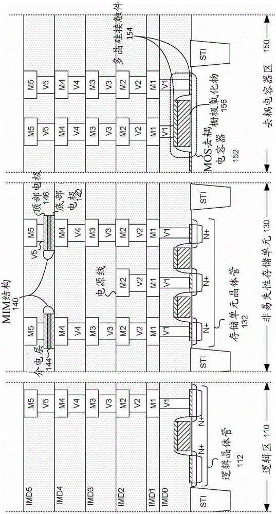
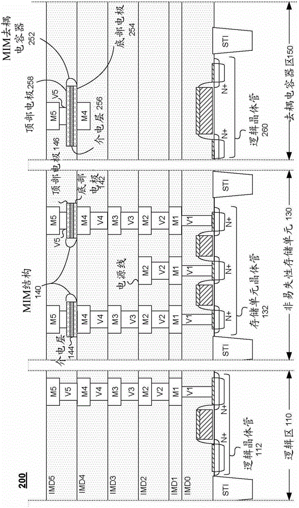
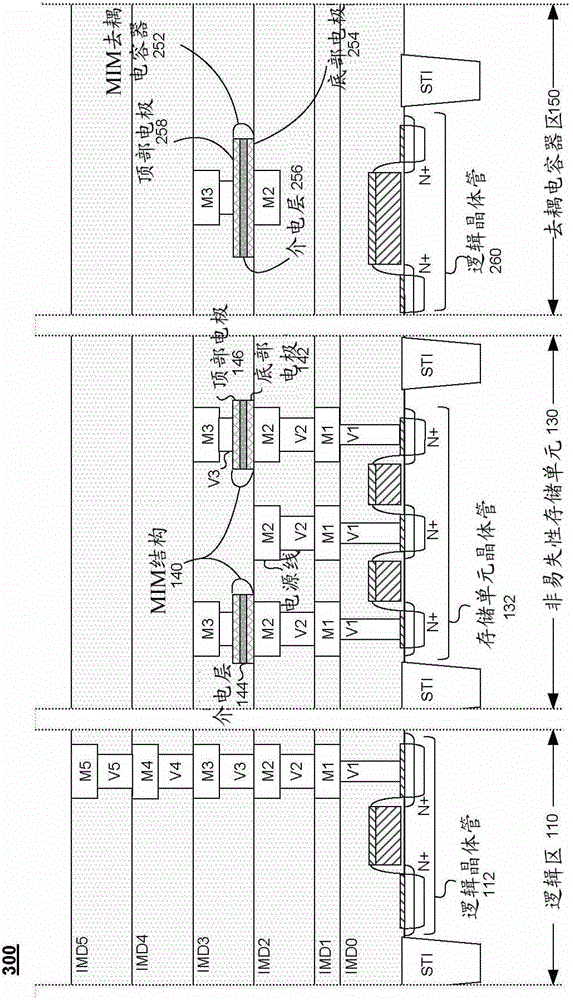
[0035] figure 1 A system-on-chip (SOC) 100 is shown, which may include multiple functional areas fabricated on a single substrate. ...


PUM


Abstract

The invention provides a process-compatible decoupling capacitor device and a manufacturing method thereof. The decoupling capacitor device includes a first dielectric layer portion deposited in a deposition process that also deposits a second dielectric layer portion for a non-volatile memory cell. Both parts are patterned using a single mask. A system-on-chip (SOC) device is also provided, the SOC includes RRAM cells and decoupling capacitors in a single intermetal dielectric layer. Methods for forming process compatible decoupling capacitors are also provided. The method includes patterning a top electrode layer, an insulating layer, and a bottom electrode layer to form a nonvolatile storage element and a decoupling capacitor.

Description

technical field [0001] The invention relates to the field of semiconductors, and more particularly, to a process-compatible decoupling capacitor and a manufacturing method thereof. Background technique [0002] The semiconductor integrated circuit industry has experienced rapid development over the past few decades. Technological advances in semiconductor materials and design have produced ever smaller and more complex circuits. These advances in materials and designs are made possible as techniques related to processing and fabrication also undergo technological advances. In the course of semiconductor development, the number of interconnected devices per unit area has increased as the smallest feature size that can be reliably manufactured decreases. [0003] Many technological advances in semiconductors have occurred in the area of ​​memory devices, some of which involve capacitors. In addition, capacitors can be used in other applications of integrated circuits (ICs),...

Claims


Application Information

Patent Timeline
Patent Type & Authority Patents(China)
IPC IPC(8): H01L23/522H01L21/768
CPCH01L23/5223H01L29/94H01L28/40H01L2924/0002H10B63/30H10B63/80H10N70/20H10N70/8833H10N70/826H10N70/063H10B12/09H10B12/50H10B12/033H01L2924/00H10B99/00H10B12/00
Inventor 涂国基朱文定
Owner TAIWAN SEMICON MFG CO LTD
Learn More