A defect scanning method based on deadly defect correction

A defect scanning and fatal defect technology, applied in electrical components, circuits, semiconductor/solid-state device testing/measurement, etc., can solve the problems of not being able to find chips, reducing product yield and production efficiency, and not being able to find machines in time. Achieve the effect of reducing ongoing impact, improving yield and production efficiency

Active Publication Date: 2014-03-19
SHANGHAI HUALI MICROELECTRONICS CORP
View PDF3 Cites 4 Cited by
  • Summary
  • Abstract
  • Description
  • Claims
  • Application Information

AI Technical Summary

Problems solved by technology

However, the above-mentioned defect scanning method has the following problems: when the number of defects on the chip does not exceed the set control standard value, because there are defects on the chip that have an important impact on its yield (such as metal corrosion, metal discharge and ion Pollution and other fatal defects), directly lead to the scrapping of the chip or shutting down the machine to clean the chip if there is such a defect on the chip, and the above defect scanning method cannot find such problems in the chip, and the product will continue to follow the production steps, resulting in problems The machine cannot be found in time, which reduces the product yield and production efficiency

Method used


Image

  • A defect scanning method based on deadly defect correction
  • A defect scanning method based on deadly defect correction

Examples


Embodiment Construction

[0022] Some typical embodiments embodying the features and advantages of the present invention will be described in detail in the description in the following paragraphs. It should be understood that the invention is capable of various changes in different examples without departing from the scope of the invention, and that the descriptions and illustrations therein are illustrative in nature rather than limiting the invention.

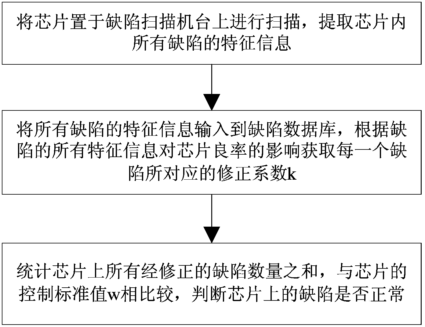
[0023] The above and other technical features and beneficial effects will be combined with the attached figure 2 A preferred embodiment of the defect scanning method based on fatal defect correction of the present invention will be described in detail.

[0024] figure 2 It is a schematic flowchart of the defect scanning method based on fatal defect correction in the present invention. see figure 2 , the defect scanning method based on fatal defect correction of the present invention will be described in detail below, which includes the following...


PUM


Abstract

The invention discloses a defect scanning method based on deadly defect correction. The defect scanning method comprises: placing a chip on a defect scanning machine table to be scanned in order to extract the characteristic information of all defects in the chip: inputting the characteristic information of all defects into a defect database in order to obtain correction coefficients k corresponding to the defects, wherein the defect database endows different correction coefficients k according to the influence of the characteristic information of all defects on the chip yield; and performing statistic on the sum of all corrected defects of the chip and comparing the sum with a control standard value w of the chip in order to determine whether the defects are normal. On the premise of determining whether the defects of the chip are normal according to the number of the defects, the defect scanning method introduces a deadly defect correction factor in order to accurately and fast determine whether the defects of the chip are normal and has advantages of fast finding machine tables having problems, decreasing continuous influence on products, and increasing product yield and production efficiency.

Description

technical field [0001] The invention relates to the technical field of integrated circuit manufacturing, in particular to a defect scanning method based on fatal defect correction. Background technique [0002] In recent years, with the rapid development of semiconductor integrated circuits and the scaling down of critical dimensions, their manufacturing processes have become increasingly complex. The current advanced integrated circuit manufacturing process generally includes hundreds of process steps, and a problem in one of the steps will cause problems in the entire semiconductor integrated circuit chip, and may even lead to the failure of the entire chip in severe cases. Based on the above considerations, the industry generally scans the defects on the chip, and judges whether the defects of the chip in production exceed the control standard according to the number of defects on the chip, and then judges whether the chip defect is normal or not. [0003] Such as figur...

Claims


Application Information

Patent Timeline
Patent Type & Authority Applications(China)
IPC IPC(8): H01L21/66
CPCH01L22/12H01L22/20
Inventor 何理许向辉郭贤权陈超
Owner SHANGHAI HUALI MICROELECTRONICS CORP
Why Eureka
Try Eureka