Realization method of automatic alarm system for semiconductor chip automatic packaging equipment

A packaging equipment, automatic alarm technology, applied in the direction of measuring devices, machine/structural components testing, instruments, etc., can solve the problems of manual search trouble, unable to find fault points, faults and abnormalities, etc., to achieve convenient, accurate and rapid positioning, It is convenient for query and management, and the effect of improving retrieval speed

Active Publication Date: 2016-04-20
安徽聚禾智能科技有限公司
View PDF6 Cites 1 Cited by
  • Summary
  • Abstract
  • Description
  • Claims
  • Application Information

AI Technical Summary

Problems solved by technology

[0004] Due to the complex structure of the fully automatic packaging equipment, it is necessary to control multiple servo motors, presses and monitor hundreds of sensors. Such a large system will inevitably have various failures during operation or system development. If the location of the failure cannot be automatically and accurately located , it is very cumbersome to search manually, and it is even impossible to find the fault point
In this way, it may be impossible to solve the problem in time due to a small fault and the failure point cannot be determined, and the system stops running.
At the same time, for a fully automatic large-scale system, there may be many faults and abnormalities, and the designer needs to fully consider the potential abnormalities. The system faces a large amount of faults and abnormal information.

Method used


Image

  • Realization method of automatic alarm system for semiconductor chip automatic packaging equipment
  • Realization method of automatic alarm system for semiconductor chip automatic packaging equipment

Examples


Embodiment Construction

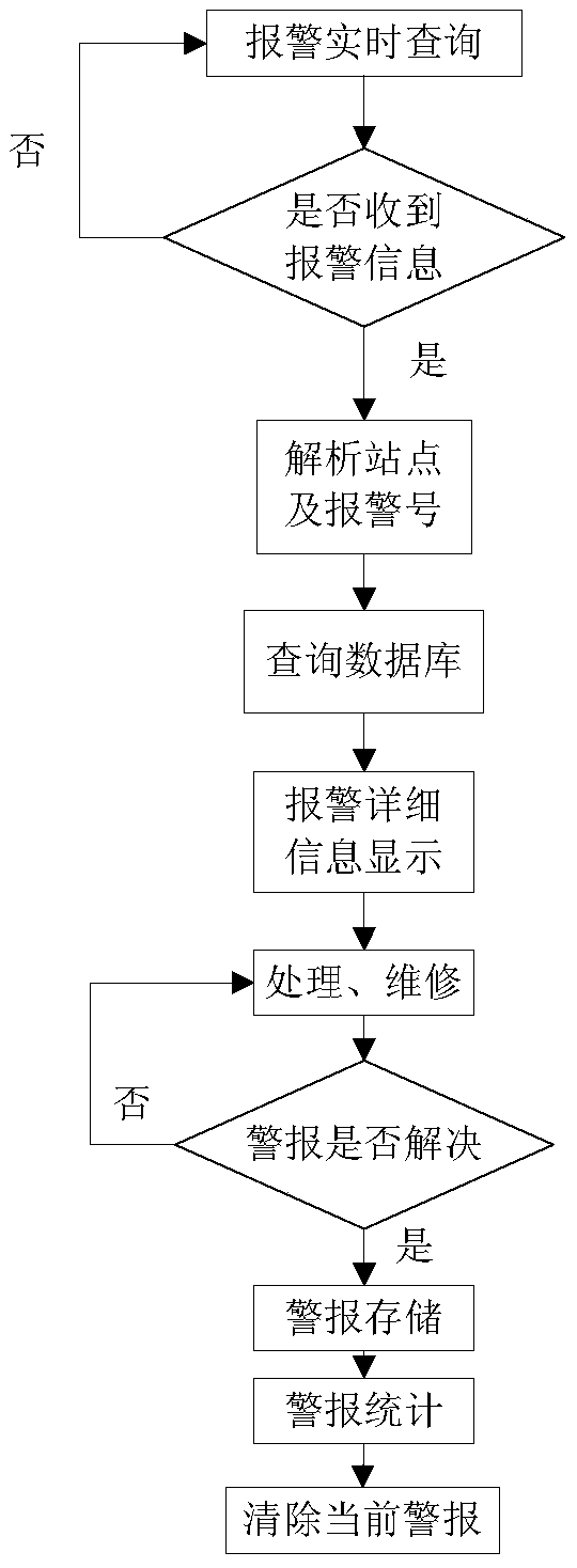
[0026] Such as figure 1 , 2 As shown, a method for realizing an automatic alarm system for a semiconductor chip fully automatic packaging equipment includes the following steps:

[0027] (1) Fault monitoring

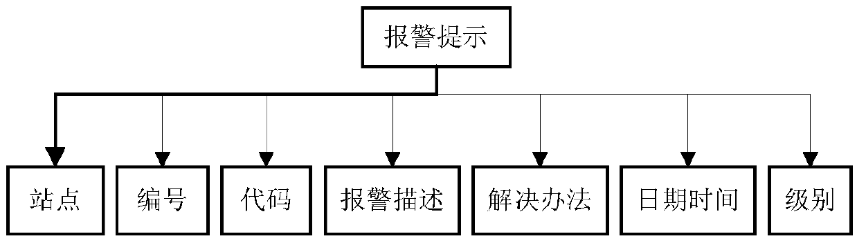
[0028] Carry out real-time monitoring of the faults of the semiconductor chip automatic packaging equipment, and find problems in time by cyclically scanning the status of each part of the system in the automatic alarm system control program. The time of each cyclic scanning should be as short as possible to avoid affecting the normal operation of the system, specifically: Divide the fault into several sites according to the fault location, each site corresponds to a relatively independent module of the automatic packaging system, and the system establishes a site fault index; if any abnormality is found during the operation of each site module, it will mark the site fault index of this site; automatically The alarm system program first cyclically scans the fault index...


PUM


Abstract

The invention discloses an automatic alarm system implementation method of semiconductor chip full-automatic packaging equipment. According to the system automatic operational process, a main program forms an overall cycle operational process. The main program invokes a module of each site in a particular sequence for automatic operation. During operational process of the module of each site, setting of fault alarm words is carried out if anything abnormal is found. A fault alarm program carries out fault scanning on each site every other 200 milliseconds. If a fault is found, the fault is parsed, fault information details are invoked from a database to be displayed on a screen, and a location map of the fault is displayed. According to the invention, abnormal and alarm information is comprehensive. Fast indexing of subsites is established, and retrieval speed is raised. The database is established for the convenience of query and management. By information grading, different handling methods are provided for different grades. Status is clear, and it is convenient to operate. By image display, it is convenient for users to position quickly.

Description

technical field [0001] The invention relates to related fields of industrial automation, in particular to the field of fully automatic industrial manufacturing equipment, and specifically relates to a method for realizing an automatic alarm system of fully automatic packaging equipment for semiconductor chips. Background technique [0002] my country's semiconductor industry has maintained a rapid development trend. However, domestic packaging companies use manual or semi-automatic packaging based on single-cylinder molds to realize a fully automated production process, which is conducive to improving production efficiency and product quality. This is the development direction of my country's packaging industry. Packaging equipment is the process from semiconductor integrated circuit to packaging production process. Fully automatic packaging equipment realizes the operation of mechanical devices through electrical and intelligent equipment without manual intervention, and co...

Claims


Application Information

Patent Timeline
Patent Type & Authority Patents(China)
IPC IPC(8): G01M99/00G06F17/30
Inventor 汪辉曹玉堂刘小勤崔利果秦来安
Owner 安徽聚禾智能科技有限公司
Why Eureka
Try Eureka