PMOLED screen splicing structure

A technology of splicing screen and screen body, applied in the direction of instruments, identification devices, etc., can solve the problems of affecting the splicing display effect, the thickness of the splicing module, and reducing the resolution, and achieve the effect of improving the resolution and display effect, and reducing the width.

Inactive Publication Date: 2014-03-26
GUAN YEOLIGHT TECH CO LTD
View PDF9 Cites 7 Cited by
  • Summary
  • Abstract
  • Description
  • Claims
  • Application Information

AI Technical Summary

Problems solved by technology

To obtain a good display effect for the splicing screen, the pixel spacing inside the screen must be consistent with the pixel spacing between the screens. However, when designing a normal PMOLED screen, in order to match the driver chip, the leads of the screen are all It is designed on one side of the screen, and the narrowest lead is about 1.5mm. Therefore, if you want to keep the pixel pitch between the screens consistent with the pixel pitch inside the screen, you can use two methods. One is to increase the pixel pitch inside the screen. , the pixel pitch of this scheme will become larger, which will directly affect the splicing display effect and reduce the resolution; another scheme is to overlap the lead area of ​​one screen with the area without lead of another spliced ​​screen, such as figure 2 As shown, but this method will cause the two screens to not be on the same plane, and the more layers are stacked, the greater the gap will be, and the entire splicing module will become very thick, which will reduce the display effect

Method used


Image

  • PMOLED screen splicing structure
  • PMOLED screen splicing structure
  • PMOLED screen splicing structure

Examples


Embodiment Construction

[0019] In order to facilitate a further understanding of the structure, method and achieved effects of the present invention, preferred embodiments are described in detail below in conjunction with the accompanying drawings.

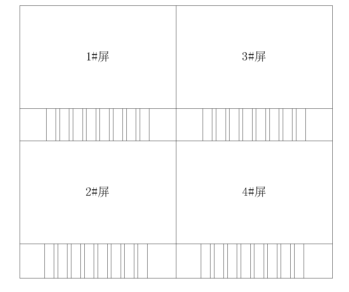
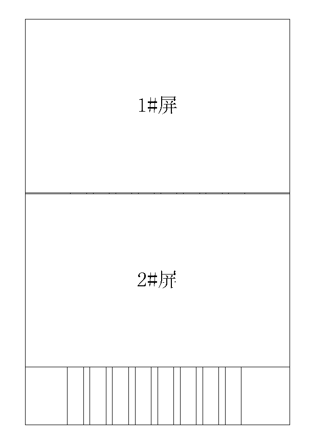
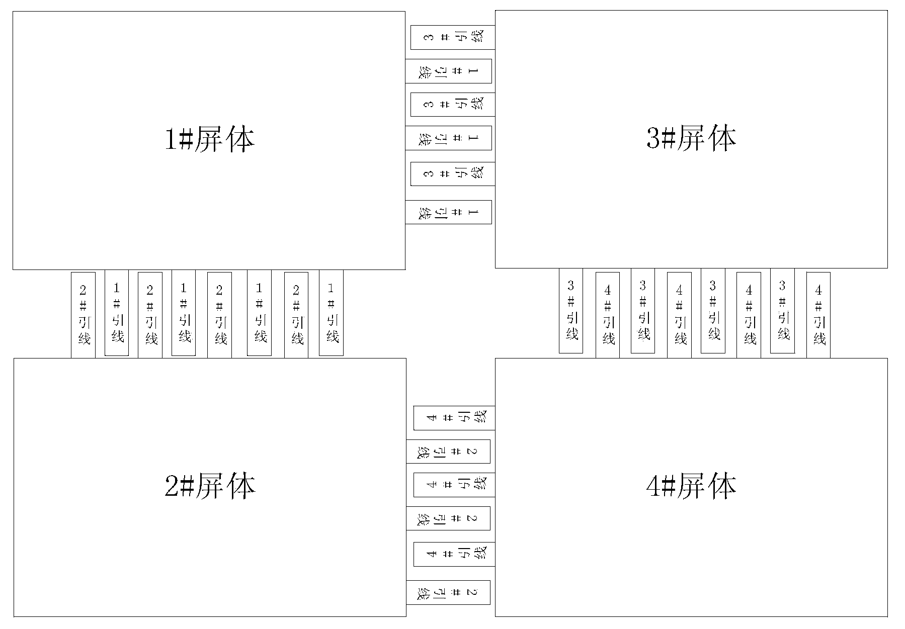
[0020] The splicing screen structure of the present invention is composed of a plurality of splicing units. When splicing the screen, such as image 3 As shown, four screens can be spliced ​​together as a splicing unit, which are 1# screen, 2# screen, 3# screen, and 4# screen. Each screen is rectangular and has the same size. The lead of each screen changes from one side to two sides, that is, there are multiple leads on the two vertical sides of each screen, and there is a certain distance between the adjacent two leads of each side. The leads at the splicing edge are cross-arranged. At the splicing edge, a certain lead of one screen is inserted between two adjacent leads of the other screen, and the adjacent two screens share the lead area. Therefore, ...


PUM


Abstract

The invention discloses a PMOLED screen splicing structure. The PMOLED screen splicing structure is formed by a plurality of splicing units. Each splicing unit is formed by splicing at least two screen bodies. The shapes and sizes of the screen bodies are the same. Edges of each screen body to be spliced in any splicing unit are provided with a plurality of leading wires. Every two leading wires on the same edge provided with the leading wires are arranged at regular intervals. The leading wires of every two adjacent screen bodies are arranged in a crossed mode on the edges to be spliced. The two adjacent screen bodies in one splicing unit share a leading wire region. The splicing units are subjected to physical arrangement to form the screen splicing structure. According to the PMOLED screen splicing structure, the two adjacent screen bodies in one splicing unit share the leading wire region, so that the width of splicing gaps is reduced and the resolution ratio and the display effect are improved.

Description

technical field [0001] The present invention relates to a PMOLED (Passive matrix Organic Light-Emitting Diode, passive organic electroluminescent diode) splicing screen structure, especially a splicing screen that can not only ensure the resolution and display effect, but also reduce the splicing gap body structure. Background technique [0002] At present, large-size and high-resolution display screens are used in some occasions. Due to the limitation of PMOLED driving methods, a single screen body cannot meet the requirements of large-size, high-resolution display. However, due to the simple process of PMOLED, The production cost is low, so multiple PMOLED screens can be spliced ​​together to achieve large-size, high-resolution display. The current method of splicing PMOLED screens is mainly to put the ready-made single PMOLED screens together directly to achieve splicing, such as figure 1 shown. To obtain a good display effect for the splicing screen, the pixel spacing...

Claims


Application Information

Patent Timeline
Patent Type & Authority Applications(China)
IPC IPC(8): G09F9/33
Inventor 张祝新
Owner GUAN YEOLIGHT TECH CO LTD
Why Eureka
Try Eureka