An electronic device containing a planar inverted F antenna with dual parasitic elements

A technology of electronic devices and parasitic components, applied to devices that enable antennas to work in different bands at the same time, antenna support/installation devices, antennas, etc., can solve problems such as antenna characteristic degradation

Active Publication Date: 2014-03-26
ACER INC
View PDF5 Cites 10 Cited by
  • Summary
  • Abstract
  • Description
  • Claims
  • Application Information

AI Technical Summary

Problems solved by technology

However, since there are usually many traces near the pivot axis, such an arrangement cannot keep the antenna away from the interference that may be caused by other components and traces at the system end, and often causes the characteristics of the antenna to degrade

Method used


Image

  • An electronic device containing a planar inverted F antenna with dual parasitic elements
  • An electronic device containing a planar inverted F antenna with dual parasitic elements
  • An electronic device containing a planar inverted F antenna with dual parasitic elements

Examples


Embodiment Construction

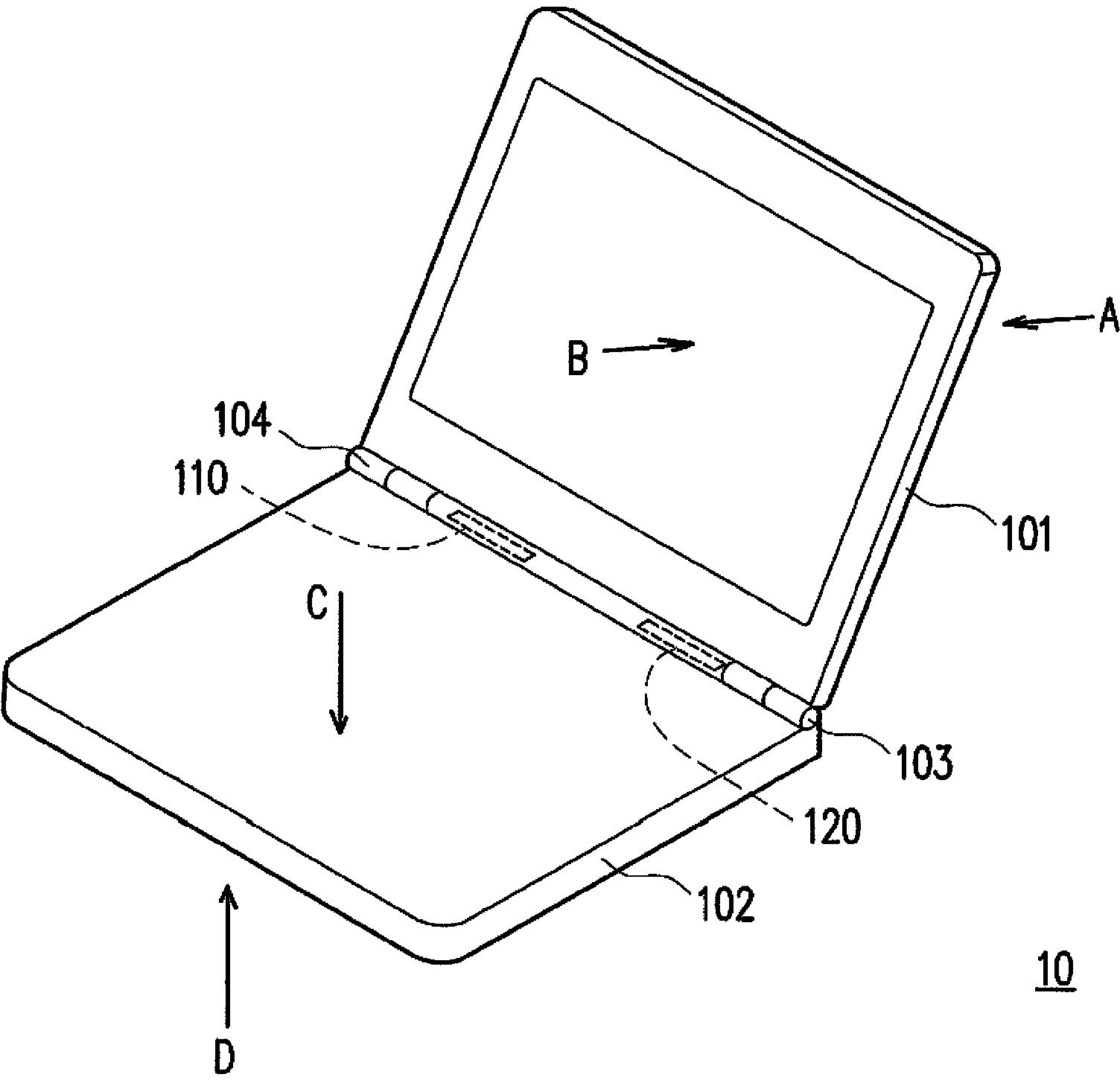
[0044] figure 1 It is a schematic diagram of an electronic device according to an embodiment of the present invention. Please refer to figure 1 , the electronic device 10 , such as a notebook computer, includes a first body 101 and a second body 102 , wherein the first body 101 is connected to the second body 102 through pivot shafts 103 , 104 and is suitable for opening and closing relative to the second body 102 . The first body 101 has an upper surface A and a lower surface B, and the second body has an upper surface C and a lower surface D.

[0045] As far as the prior art is concerned, the antenna is often disposed on the first body 101 . However, when the upper surface A of the first body 101 and the upper surface C of the second body are made of metal materials, the antenna transceiving capability will be shielded by the metal and cannot be installed. If further, when the upper surface A of the first body 101, the upper surface C and the lower surface D of the second...


PUM


Abstract

The invention provides an electronic device containing a planar inverted F antenna with dual parasitic elements. The planar inverted F antenna comprises an antenna body, a grounding element, a low-frequency parasitic portion, and a high-frequency parasitic portion. The antenna body comprises a high-frequency radiation portion, a low-frequency radiation portion, and a connection portion. The high-frequency radiation portion and the low-frequency radiation portion are extended along opposite directions. The connection portion comprises a first end, a second end, and a feed-in point. The first end is coupled to a joint of the high-frequency radiation portion and the low-frequency radiation portion. The second end is coupled to the grounding element. The feed-in point is used for receiving a signal input. The grounding element is connected with the second end of the connection portion of the antenna body. The low-frequency parasitic portion is extended from the grounding element and is adjacent to the high-frequency radiation portion of the antenna body. The high-frequency parasitic portion extended from the grounding element is arranged between the antenna body and the low-frequency parasitic portion and is adjacent to the connection portion and the high-frequency radiation portion of the antenna body.

Description

technical field [0001] The present invention relates to an electronic device, and in particular to an electronic device having a planar inverted-F antenna with dual parasitic elements. Background technique [0002] With the rapid development of technology, the volume and size of handheld electronic devices are also developing towards thinner, lighter and smaller. While the product is pursuing light weight and miniaturization, the space available for the antenna for sending and receiving communication signals will inevitably be compressed. Coupled with the limitation of physical conditions, the characteristics of the antenna are greatly affected. For example, the placement position of the antenna in a general traditional notebook computer is mostly above the screen. However, in the evolution of notebook computers in pursuit of lightness, lightness and compactness, the back cover is often covered with all-metal materials. In such a case, the antenna is forced to be placed o...

Claims


Application Information

Patent Timeline
Patent Type & Authority Applications(China)
IPC IPC(8): H01Q1/36H01Q1/52H01Q1/22H01Q5/01G06F1/16H01Q5/10
Inventor 杨崇文
Owner ACER INC
Why Eureka
Try Eureka