Camera module, and encapsulating structure and encapsulating method thereof

A camera module and packaging structure technology, which is applied in the direction of TV, color TV, electrical components, etc., can solve the problems of large closed space, unfavorable production efficiency, falling off, etc., achieve good image quality, save materials and resources, and improve production efficiency high effect

Active Publication Date: 2014-04-02
NANCHANG OFILM HUAGUANG TECH CO LTD
View PDF5 Cites 87 Cited by
  • Summary
  • Abstract
  • Description
  • Claims
  • Application Information

AI Technical Summary

Problems solved by technology

The camera modules in the prior art have the following defects: 1) In the packaging structure, the closed space formed by the circuit board 1, the support 4 and the infrared filter 5 is relatively large, and it is easy to fall into and retain dust. When the dust enters the image sensor 2) the passive element 3 is exposed in the closed space and is prone to fall off; 3) the infrared filter 5 needs to have a larger size to cover the image sensing area. On the sensing area 21 of the measuring chip, it is usually about 2-3mm larger than the sensing area 21 of the image sensing chip on a single side, resulting in waste of materials and increased cost; 4) When the image sensing chip 2 uses a 5M or 8M COMS For the photosensitive chip, the support 4 is usually common, so the infrared filter 5 for the 5M or 8M COMS photosensitive chip is also common, and its size is 6.2mm×6.2mm, and the infrared filter 5 of this size is used When using a 5M COMS photosensitive chip, the area of ​​the non-filtering area will be large, resulting in a huge waste of materials and resources; 5) The packaging structure usually needs to be manufactured individually, and the process is complicated, which is not conducive to improving production efficiency

Method used


Image

  • Camera module, and encapsulating structure and encapsulating method thereof
  • Camera module, and encapsulating structure and encapsulating method thereof
  • Camera module, and encapsulating structure and encapsulating method thereof

Examples


Embodiment Construction

[0041] In order to make the purpose, technical solutions and advantages of the present invention clearer, the technical solutions in the embodiments of the present invention will be clearly and completely described below in conjunction with the accompanying drawings. Obviously, the described embodiments are part of the embodiments of the present invention, rather than Full examples. Based on the embodiments of the present invention, all other embodiments obtained by persons of ordinary skill in the art without making creative efforts belong to the protection scope of the present invention.

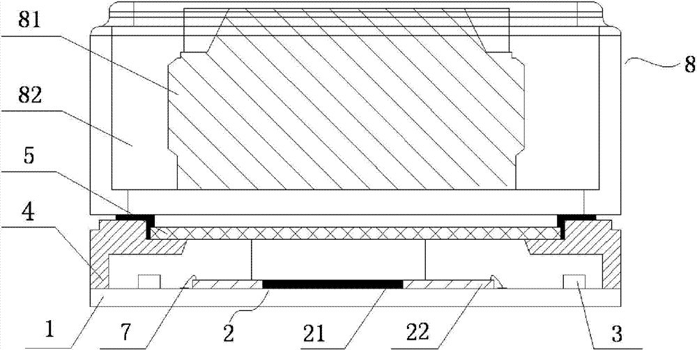
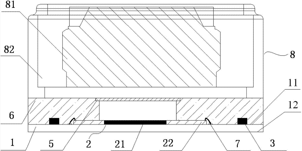
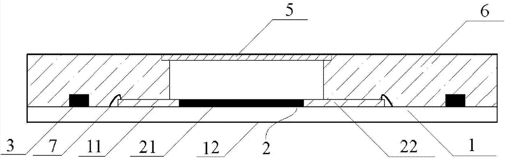
[0042] figure 2It is a schematic structural diagram of a camera module according to an embodiment of the present invention, the camera module includes a camera module packaging structure, a lens module 8 and a flexible circuit board (not shown in the figure); wherein the packaging structure includes a circuit board 1, an image Sensing chip 2, passive element 3, infrared filter 5 and pack...


PUM


Abstract

The invention provides a camera module, and an encapsulating structure and an encapsulating method thereof. The encapsulating structure of the camera module comprises a circuit board, an image sensing chip, a passive element, an encapsulating part and an infrared filter, wherein the circuit board is provided with a first surface and a second surface; the image sensing chip and the passive element are arranged on the first surface of the circuit board, and the image sensing chip is provided with a sensing region and a non-sensing region and electrically connected with the circuit board; the encapsulating part is arranged on the first surface of the circuit board and at least part of the non-sensing region of the image sensing chip and encompasses the passive element; the infrared filter is arranged on the encapsulating part and located in a position above the sensing region of the image sensing chip, and forms an enclosure space together with the encapsulating part and the sensing region of the image sensing chip. The infrared filter of the encapsulating structure of the camera module is smaller in size so as to facilitate material saving and cost reduction; besides, impurities such as dust are unlikely to fall or be left in the enclosure space, so that the imaging quality is high.

Description

technical field [0001] The present invention relates to a packaging structure, in particular to a camera module and its packaging structure and packaging method. Background technique [0002] figure 1 It is a schematic structural diagram of a camera module in the prior art. Such as figure 1 As shown, the camera module in the prior art includes a packaging structure and a lens module 8, wherein the packaging structure includes a circuit board 1, an image sensing chip 2, a passive component 3 (that is, a passive component, such as a capacitor, a resistor), a support seat 4 and infrared filter 5, wherein the image sensing chip 2, the passive element 3 and the support 4 are all arranged on the circuit board 1, the image sensing chip 2 has a sensing area 21 and a non-sensing area 22, and its The metal wire 7 is electrically connected to the circuit board 1, and the infrared filter 5 is arranged on the support 4 and corresponds to the sensing area 21 of the image sensing chip; ...

Claims


Application Information

Patent Timeline
Patent Type & Authority Applications(China)
IPC IPC(8): H01L23/31H04N5/225
Inventor 齐书
Owner NANCHANG OFILM HUAGUANG TECH CO LTD
Why Eureka
Try Eureka