
Display panel

一种显示面板、显示区的技术,应用在静态指示器、仪器、非线性光学等方向,能够解决GOA元件无法设计得太密集、显示面板窄边框目的无法实现等问题,达到缩小边框的效果

Active Publication Date: 2014-04-30
AU OPTRONICS CORP
View PDF3 Cites 20 Cited by
  • Summary
  • Abstract
  • Description
  • Claims
  • Application Information

AI Technical Summary

Problems solved by technology

However, the GOA at the place where the sealant is located is designed with opaque metal so that the GOA components cannot be designed too densely, which leads to the failure of the narrow frame of the display panel.

Method used


Image

  • Display panel
  • Display panel
  • Display panel

Examples


no. 1 example

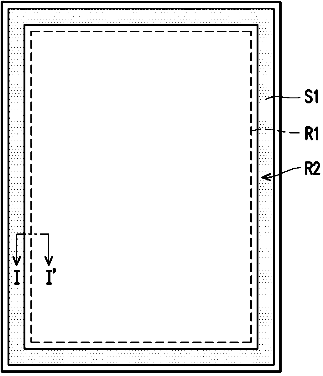
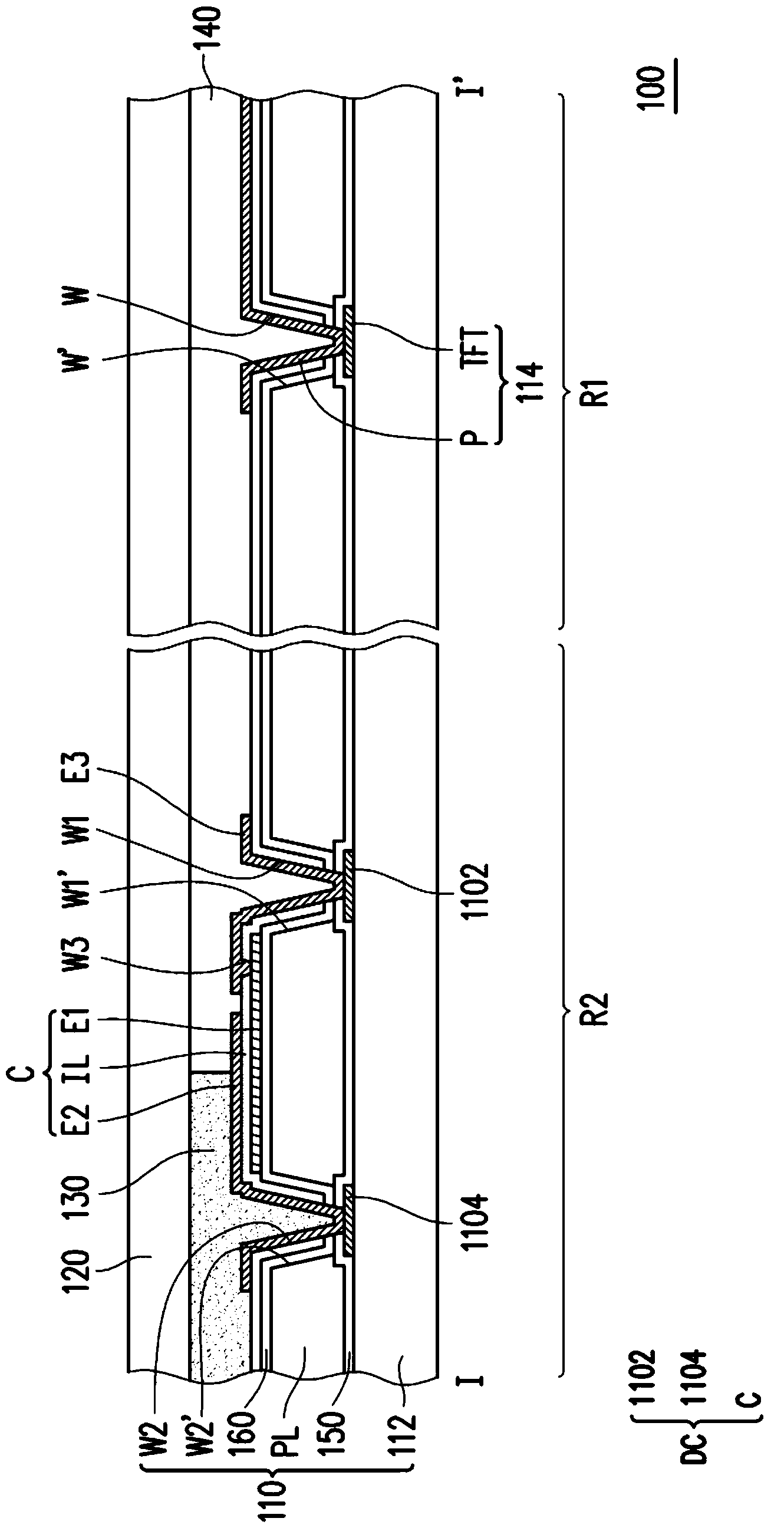
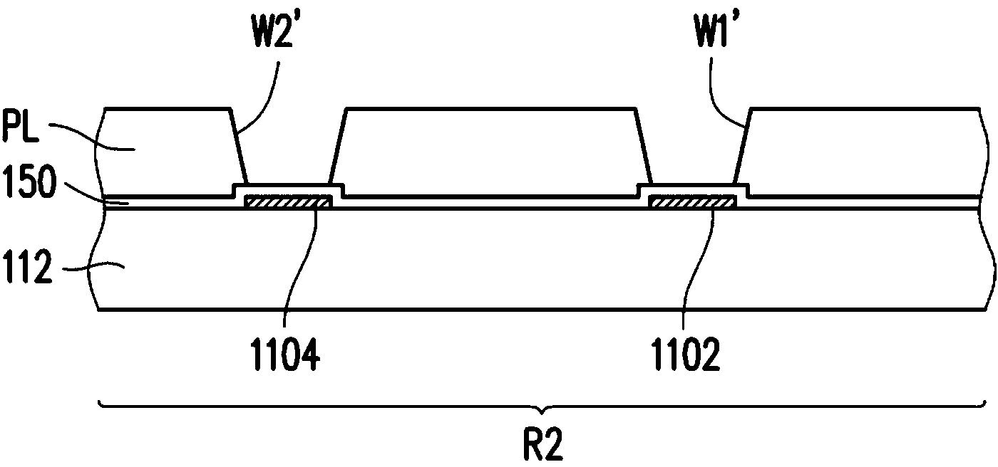
[0060] figure 2 is along figure 1 A partial cross-sectional view of the first embodiment of the present invention shown by the line I-I' of the display panel. Please refer to figure 1 and figure 2, in this embodiment, the display panel 100 includes an active array substrate 110 , an opposite substrate 120 , a sealant 130 and a display medium 140 . The opposite substrate 120 is disposed opposite to the active array substrate 110 . The active array substrate 110 includes a substrate 112 , a pixel array 114 and a driving circuit DC disposed on the substrate 112 . The substrate 112 can be a rigid substrate or a flexible substrate, and its material can be glass, quartz, organic polymer or other suitable materials. The pixel array 114 is located in the display area R1, and the driving circuit DC is located in the non-display area R2. The pixel array 114 includes a thin film transistor (thin film transistor, TFT) array and a pixel electrode P electrically connected to the thi...

no. 2 example

[0078] Figure 4 is along figure 1 A partial cross-sectional view of the second embodiment of the present invention shown by the line I-I' of the display panel. The second embodiment is similar to the above-mentioned first embodiment, so the same or similar elements are denoted by the same or similar symbols, and the description will not be repeated. The main difference between the display panel 200 and the display panel 100 is that there is no protective layer 160 between the insulating layer PL and the first transparent electrode layer E1 of the display panel 200 . It is worth mentioning that, in this embodiment, the insulating layer PL is first patterned using a photomask to form openings W', W1', W2', and then another photomask is used to pattern the dielectric layer IL. The passivation layer 150 is subjected to a photolithography process and a corresponding etching procedure to form the opening W, the first opening W1 , the second opening W2 and the contact opening W3 ....

no. 3 example

[0084] Figure 6 is along figure 1 The partial cross-sectional view of the third embodiment of the present invention shown by the line I-I' of the display panel. The third embodiment is similar to the above-mentioned first embodiment, so the same or similar elements are denoted by the same or similar symbols, and the description will not be repeated. The main difference between the display panel 300 and the display panel 100 is that there is no protective layer 150 on the first conductive element 1102 and the second conductive element 1104 of the display panel 300, that is, the insulating layer PL is directly located on the first conductive element 1102 and the second conductive element 1104. on the conductive element 1104 . Similarly, the dielectric layer IL and the passivation layer 160 have a first opening W1 and a second opening W2 in common. In addition, the dielectric layer IL also has a contact opening W3, wherein the first opening W1 and the second opening W2 respect...


PUM


Abstract

The present invention discloses a display panel, having a display region and a non-display region. The display panel comprises an active array substrate and an opposite substrate arranged opposite to the active array substrate. The active array substrate comprises a substrate, a pixel array, and a driving circuit. The pixel array and the driving circuit are arranged on the substrate, the pixel array is arranged in the display region, and the driving circuit is arranged in the non-display region. The driving circuit comprises a first transmitting electrode layer, a second transmitting electrode layer and a dielectric layer. The dielectric layer is arranged between the first transmitting electrode layer and the second transmitting electrode layer, wherein the first transmitting electrode layer and the second transmitting electrode layer are electrically coupled to each other, so as to form at least one transmitting capacitor.

Description

technical field [0001] The present invention relates to a display panel, and in particular to a display panel with a driving circuit structure. Background technique [0002] In recent years, with the advancement of technology and the increasing development of the semiconductor industry, users' demand for digital products is also increasing. Display screens, which play an important role in digital products, have therefore become the focus of developers. Among them, liquid crystal display A panel (liquid crystal display panel, LCD panel) is a mainstream display screen. [0003] Generally speaking, in the liquid crystal display panel, the element substrate and the opposite substrate are assembled together through a sealant, and a liquid crystal layer is injected between the element substrate and the opposite substrate. The element substrate can be an active array substrate or a passive array substrate, and the opposite substrate can be a common blank substrate or a substrate p...

Claims


Application Information

Patent Timeline
Patent Type & Authority Applications(China)
IPC IPC(8): G02F1/133
CPCG02F1/1339G02F1/13454G02F1/134372G02F1/133345G02F1/134309G02F1/13439G02F1/136213G02F1/136227G02F1/1368
Inventor 黄德群黄国有黄郁涵蔡易积
Owner AU OPTRONICS CORP
Learn More