Camera Link interface testing and developing system based on FPGA

A technology for developing systems and interfaces, which is applied to components of TV systems, components of color TVs, TVs, etc.

Inactive Publication Date: 2014-04-30
KUNMING UNIV OF SCI & TECH
View PDF4 Cites 14 Cited by
  • Summary
  • Abstract
  • Description
  • Claims
  • Application Information

AI Technical Summary

Problems solved by technology

However, there is currently no learning product that takes into account both FPGA and Camera Link technologies in the market

Method used


Image

  • Camera Link interface testing and developing system based on FPGA
  • Camera Link interface testing and developing system based on FPGA
  • Camera Link interface testing and developing system based on FPGA

Examples


Embodiment 1

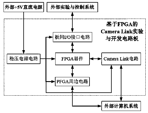
[0030] Embodiment 1: as Figure 1-2 Shown, a kind of Camera Link interface experiment and development system based on FPGA, comprise a Camera Link interface experiment and development circuit board based on FPGA, described Camera Link interface experiment and development circuit board based on FPGA comprise FPGA device, FPGA peripheral circuit , inter-board I / O interface circuit, Camera Link circuit and regulated power supply circuit; the described Camera Link interface experiment based on FPGA and the regulated power supply circuit on the development circuit board are connected with external +5V DC power supply, in the FPGA peripheral circuit The JTAG interface and AS interface are connected to the USB interface of the external computer system through the USB download cable, the Camera Link circuit is connected to the Camera Link image acquisition card in the external computer system through the Camera Link cable, and the I / O interface circuit between the boards is connected t...

Embodiment 2

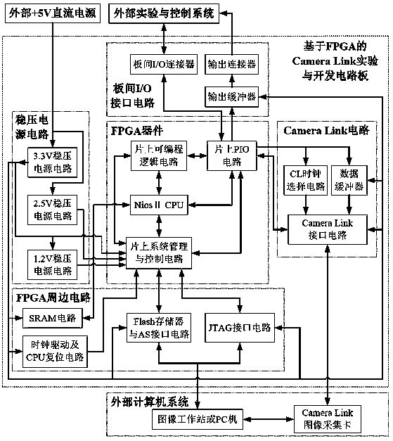
[0038] Embodiment 2: as figure 1 image 3 Shown, a kind of Camera Link interface experiment and development system based on FPGA, comprise a Camera Link interface experiment and development circuit board based on FPGA, described Camera Link interface experiment and development circuit board based on FPGA comprise FPGA device, FPGA peripheral circuit , inter-board I / O interface circuit, Camera Link circuit and regulated power supply circuit; the described Camera Link interface experiment based on FPGA and the regulated power supply circuit on the development circuit board are connected with external +5V DC power supply, in the FPGA peripheral circuit The JTAG interface and AS interface are connected to the USB interface of the external computer system through the USB download cable, the Camera Link circuit is connected to the Camera Link image acquisition card in the external computer system through the Camera Link cable, and the inter-board I / O interface circuit is connected t...

Embodiment 3

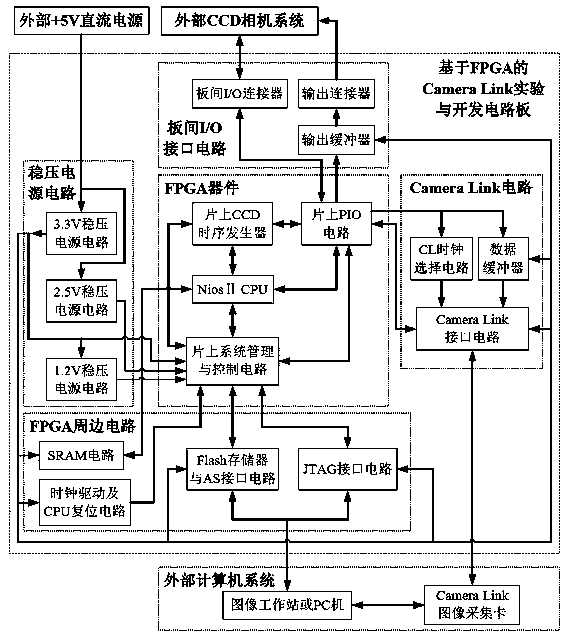
[0046] Embodiment 3: as figure 1 Figure 4 Shown, a kind of Camera Link interface experiment and development system based on FPGA, comprise a Camera Link interface experiment and development circuit board based on FPGA, described Camera Link interface experiment and development circuit board based on FPGA comprise FPGA device, FPGA peripheral circuit , inter-board I / O interface circuit and regulated power supply circuit; the described Camera Link interface experiment based on FPGA and the regulated power supply circuit on the development circuit board are connected with external +5V DC power supply, the JTAG interface and in the FPGA peripheral circuit The AS interface is connected to the USB interface of the external computer system through the USB download cable, and the inter-board I / O interface circuit is connected to the external experiment and control system.

[0047] The internal circuit of the FPGA device includes an on-chip system management and control circuit, an o...


PUM


Abstract

The invention relates to a Camera Link interface testing and developing system based on the FPGA, and belongs to the technical field of digital logic design and high speed data transmission. The Camera Link interface testing and developing system based on the FPGA comprises a Camera Link interface testing and developing circuit board based on the FPGA, wherein the circuit board comprises an FPGA component, an FPGA peripheral circuit, a Camera Link circuit, an inter-board I / O interface circuit and a voltage-stabilized source circuit. The Camera Link interface testing and developing system is connected with an external computer through a Camera Link interface cable to be used as a testing platform of an embedded system for learning Camera Link camera control and Channel Link high speed data transmission based on the FPGA or used as a development board of a real CCD camera system; the Camera Link interface testing and developing system can also be connected with the computer through a USB download cable to be used as a testing circuit board for learning the FPGA programming and application technology or used as a development board of a real FPGA application system.

Description

technical field [0001] The invention relates to an FPGA-based Camera Link interface experiment and development system, especially suitable for FPGA-based Camera Link interface experiment and application development, and belongs to the technical field of digital logic design and high-speed data transmission. Background technique [0002] Camera Link is a high-speed image data transmission protocol. It is a communication interface technical standard for machine vision applications jointly proposed by NI, camera equipment suppliers, and some image acquisition companies at the beginning of this century. Using this protocol can simplify the image acquisition interface, making the connection between the camera and the data acquisition card more convenient. Camera Link interface is developed on the basis of Channel Link transmission technology. Channel Link technology is a technology developed by National Semiconductor Corporation based on low-voltage differential signaling (LVDS)...

Claims


Application Information

Patent Timeline
Patent Type & Authority Applications(China)
IPC IPC(8): H04N17/00H04N5/77
Inventor 李彬华卢家莉刘玲李达伦
Owner KUNMING UNIV OF SCI & TECH
Why Eureka
Try Eureka