Image sensor pixel structure for preventing image dispersion and manufacturing method thereof

An image sensor and pixel structure technology, applied in radiation control devices and other directions, can solve the problems of increasing the number of saturated pixels, unable to reflect pixel signals, and reducing image quality, and achieve the effect of eliminating pixel color distortion and preventing image dispersion.

Active Publication Date: 2017-02-15
BEIJING SUPERPIX MICRO TECHNOLOGY CO LTD
View PDF4 Cites 0 Cited by
  • Summary
  • Abstract
  • Description
  • Claims
  • Application Information

AI Technical Summary

Problems solved by technology

This will make the crosstalked pixel signal unable to reflect the real light, cause the number of saturated pixels to increase than the actual one, and cause image color distortion and image dispersion phenomenon
Therefore, the image sensor with image dispersion phenomenon cannot correctly collect the object information near the strong light object, thereby reducing the quality of the image

Method used


Image

  • Image sensor pixel structure for preventing image dispersion and manufacturing method thereof
  • Image sensor pixel structure for preventing image dispersion and manufacturing method thereof
  • Image sensor pixel structure for preventing image dispersion and manufacturing method thereof

Examples


Embodiment 1

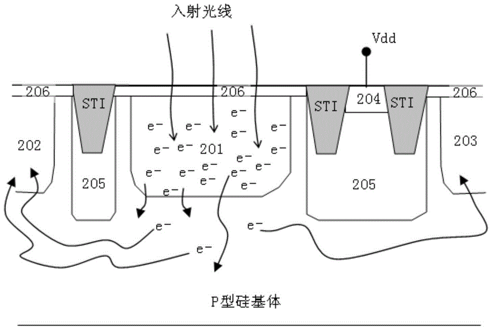
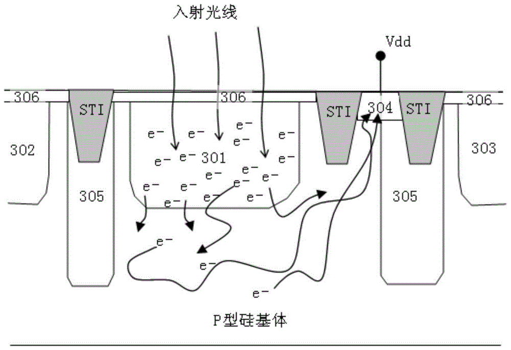
[0031] An embodiment of the present invention provides an image sensor pixel structure for preventing image dispersion, which at least includes a photodiode placed in a semiconductor substrate, a shallow trench isolation region arranged on one side of the photodiode, and a shallow trench isolation region arranged on the other side of the photodiode. Two shallow trench isolation regions and a transistor drain active region disposed between the two shallow trench isolation regions and connected to the power supply, wherein one shallow trench isolation region on one side of the photodiode, and one on the other side A deep P-type well region is provided on one of the two shallow trench isolation regions and part of the active region (not fully covered) at the drain end of the transistor, wherein the active region on the drain end of the transistor A deep P-type well region, which covers the shallow trench isolation region farther from the photodiode, and is not in contact with the ...

Embodiment 2

[0041] An embodiment of the present invention provides a method for manufacturing a pixel structure of an image sensor that prevents image dispersion. The specific process steps include Figure 4 ~ Figure 7 Steps shown:

[0042] 1) if Figure 4 As shown, after the STI process in the traditional CMOS process, an oxide layer 401 is grown on the surface of the semiconductor substrate as a process protection layer with a thickness of 10nm-12nm. This embodiment uses a P-type silicon substrate.

[0043] 2) if Figure 5 As shown, the photoresist is spin-coated and developed to open the predetermined P-type well injection region; the thickness of the photoresist is not less than 2.7um. The opening in the predetermined P-type well injection region includes: an opening facing a shallow trench isolation region on one side of the photodiode, another opening covering the shallow trench isolation region and part of the active region away from the photodiode, and not make contact with th...


PUM


Abstract

The invention discloses an image sensor pixel structure for preventing image diffusion and a manufacturing method thereof, wherein a shallow slot isolation region on one side of a photodiode of the image sensor pixel structure, one of two shallow slot isolation regions on the other side of the photodiode and an active region at a drain terminal part of a transistor are respectively provided with a deep P-type well region, wherein the deep P-type well region on the active region at the drain terminal of the transistor covers the shallow slot isolation region which is far away from the photodiode and is not in contact with the shallow slot isolation region which is close to the photodiode, so that an overflow charge current guide channel is formed between the photodiode and the active region at the drain terminal of the transistor. By adopting the image sensor pixel structure and the manufacturing method thereof disclosed by the invention, diffusion phenomenon of the acquired image can be prevented, and the problem of color distortion of surrounding pixels of an intense-light image is also eliminated.

Description

technical field [0001] The invention relates to the technical field of semiconductor manufacturing, in particular to an image sensor pixel structure for preventing image dispersion and a manufacturing method thereof. Background technique [0002] Image sensors have been widely used in digital cameras, mobile phones, medical devices, automobiles and other applications. In particular, the rapid development of CMOS (Complementary Metal Oxide Semiconductor) image sensor technology has made people have higher requirements for the output image quality of image sensors. [0003] In the image sensor chip in the prior art, the bright spots or bright line areas in the collected images are larger than the actual object image size. For example, when the photos taken contain bright objects such as the sun, car headlights, incandescent lamps, or strong reflections, these objects will be larger than the actual size, and the bright areas such as the sun and lights will become much larger t...

Claims


Application Information

Patent Timeline
Patent Type & Authority Patents(China)
IPC IPC(8): H01L27/146
Inventor 郭同辉陈杰刘志碧唐冕旷章曲
Owner BEIJING SUPERPIX MICRO TECHNOLOGY CO LTD
Why Eureka
Try Eureka