An image sensor pixel structure for preventing image dispersion and its manufacturing method
An image sensor and pixel structure technology, applied in the field of semiconductors, can solve the problems of inability to reflect pixel signals, increase the number of saturated pixels, reduce image quality, etc., and achieve the effect of preventing image dispersion and eliminating pixel color distortion
- Summary
- Abstract
- Description
- Claims
- Application Information
AI Technical Summary
Problems solved by technology
Method used
Image
Examples
Embodiment 1
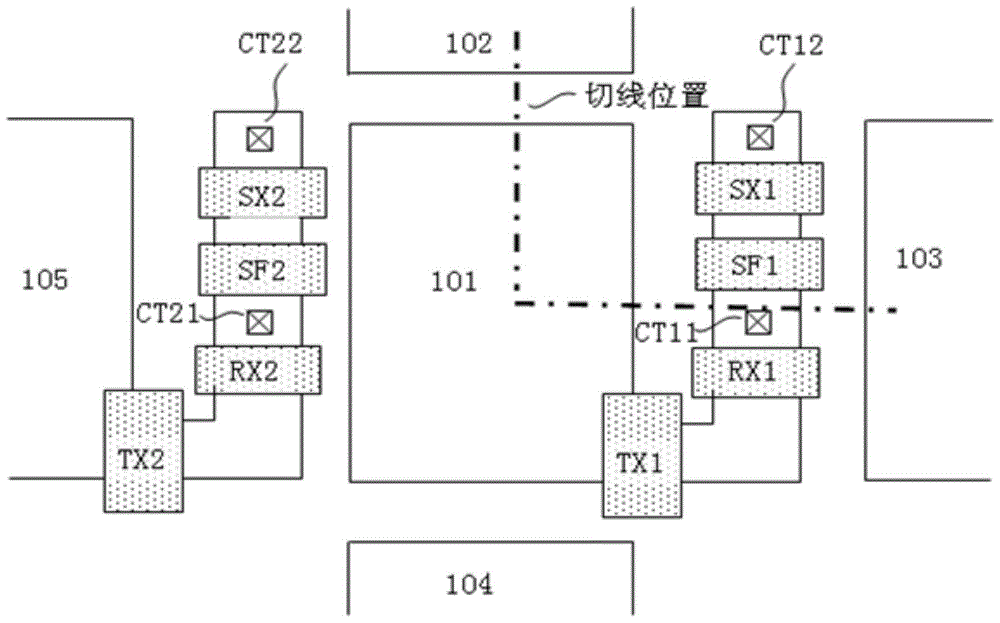
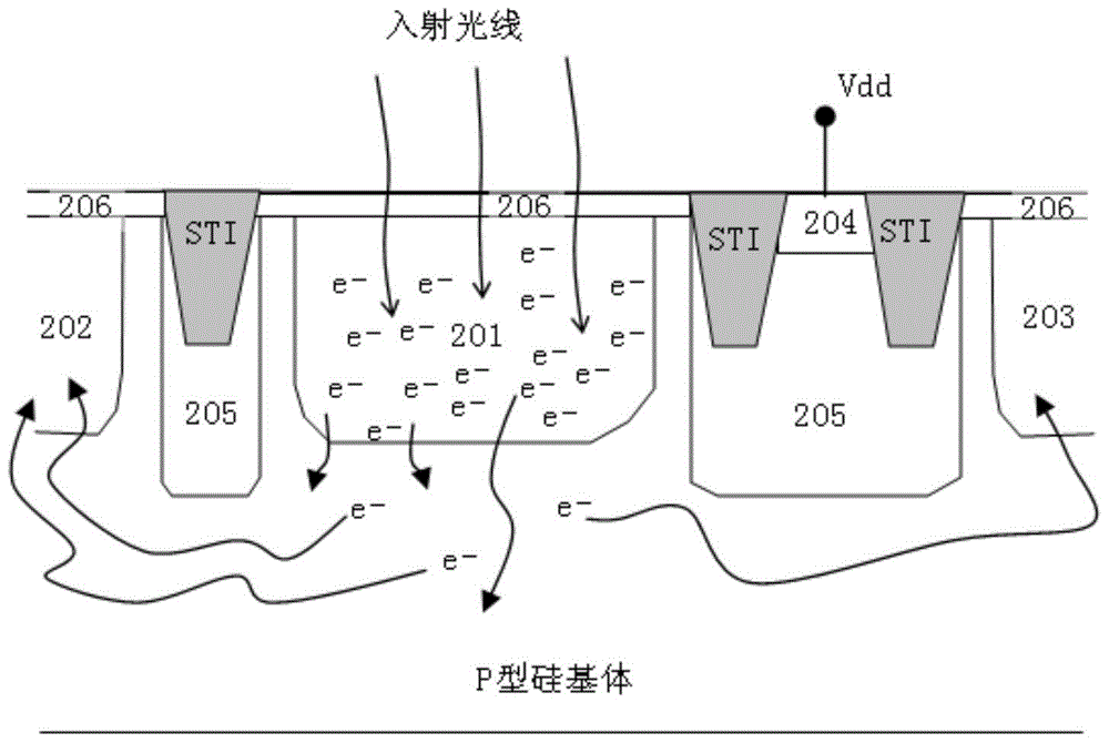
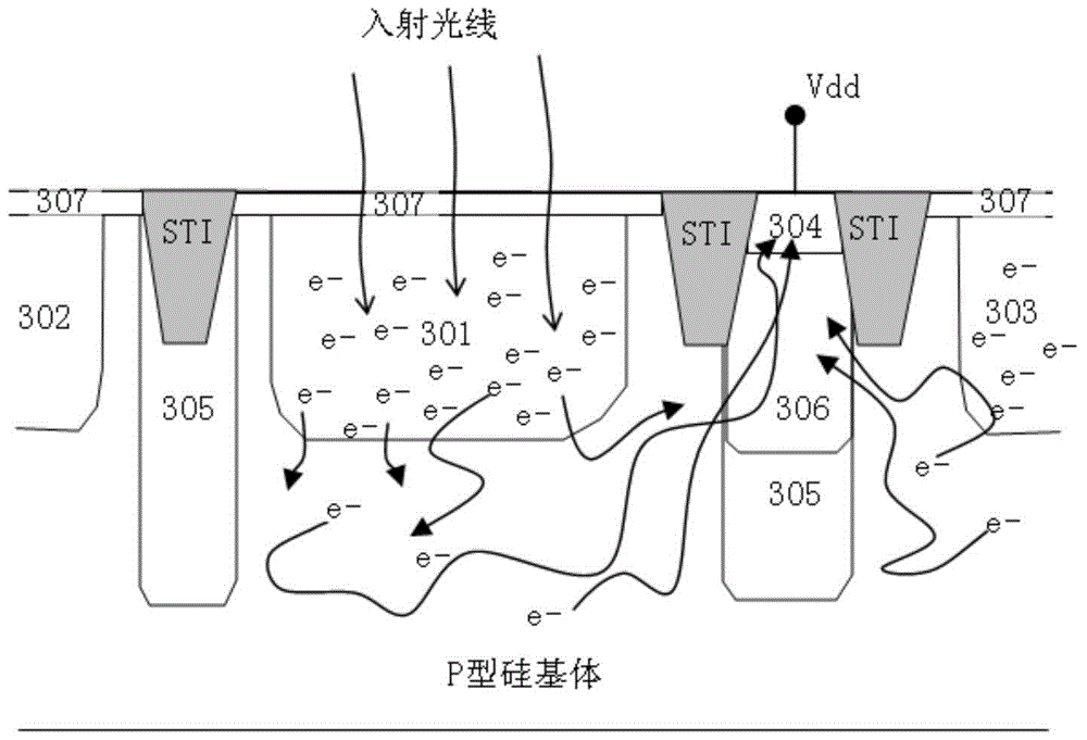
[0042] An embodiment of the present invention provides an image sensor pixel structure for preventing image dispersion, at least including a photodiode placed in a semiconductor substrate, a shallow trench isolation region arranged on one side of the photodiode, and a shallow trench isolation region arranged on the other side of the photodiode The two shallow trench isolation regions and the transistor drain active region disposed between the two shallow trench isolation regions and connected to the power supply, wherein a shallow trench isolation region on one side of the photodiode is provided with a deep P N-type well region; the transistor drain active region is sequentially provided with an N-type well region and a deep P-type well region, so that there is an overflow charge conduction channel between the transistor drain active region and the adjacent photodiodes on both sides .
[0043] Further, the depth of the N-type well region is 0.5um˜1.5um.
[0044] Further, the de...
Embodiment 2
[0054] An embodiment of the present invention provides a method for manufacturing a pixel structure of an image sensor that prevents image dispersion. The specific process steps include Figure 4 ~ Figure 10 Steps shown:
[0055] 1) if Figure 4 As shown, after the STI (Shallow Trench Isolation) process in the traditional CMOS process, an oxide layer 401 is grown on the surface of the semiconductor substrate as a process protection layer with a thickness of 10nm-12nm. This embodiment uses a P-type silicon substrate .
[0056] 2) if Figure 5 As shown, the photoresist is spin-coated and developed to open the predetermined P-type well injection region; the thickness of the photoresist is not less than 2.7um. The opening in the predetermined P-type well injection region includes: an opening facing a shallow trench isolation region on one side of the photodiode, and another opening facing the transistor between the two shallow trench isolation regions on the other side of the ...
PUM
 Abstract
Description
Claims
Application Information


