Surface acoustic wave device

a surface acoustic wave and waveguide technology, applied in piezoelectric/electrostrictive/magnetostrictive devices, piezoelectric/electrostriction/magnetostriction machines, impedence networks, etc., can solve the problem of insufficient stop band, inability to use resonators practically, and inability to achieve sufficient stop band, etc. problem, to achieve the effect of superior resonant properties and filter properties

Active Publication Date: 2008-02-05
MURATA MFG CO LTD
View PDF19 Cites 103 Cited by
  • Summary
  • Abstract
  • Description
  • Claims
  • Application Information

AI Technical Summary

Benefits of technology

[0013]To overcome the problems described above, preferred embodiments of the present invention provide a surface acoustic wave device in which an insulating layer is formed on an electrode and in which the properties are not degraded by ripples which appear, for example, in resonant properties. That is, a surface acoustic wave device is provided which has superior resonant properties and filter properties.
[0026]In the surface acoustic wave device according to preferred embodiments of the present invention, on the piezoelectric substrate, the electrode is preferably composed of a metal having a density higher than that of Al, an alloy primarily composed of the metal, or a laminate having a metal layer composed of a metal having a density higher than that of Al or an alloy primarily composed of the metal, the first SiO2 layer having a thickness approximately equal to that of the electrode is disposed in a remaining area other than that at which the electrode is provided, and the second SiO2 layer is disposed so as to cover the electrode and the first SiO2 layer. In the surface acoustic wave device described above, the density of the electrode is preferably set to at least about 1.5 times that of the first SiO2 layer. Thus, when the upper surface of the second SiO2 layer is planarized, ripples which appear in resonant properties and / or filter properties are moved out of the band, and in addition, the ripples are prevented and minimized. In addition, superior frequency-temperature properties are achieved.
[0027]In addition, since the silicon nitride compound layer is disposed on the second SiO2 layer, the properties can be adjusted and improved. Furthermore, by performing dry etching of the SiN, the frequency can be adjusted without changing TCF and the fractional band width.
[0028]In addition, in the case in which 0.08≦h / λ≦0.5 is satisfied, where the thickness of the second SiO2 film is represented by h, and the wavelength of a surface acoustic wave is represented by λ, as will be apparent from experimental results described below, the frequency-temperature properties TCF is improved. That is, the absolute value of TCF is decreased.
[0030]Furthermore, in the case in which 0.005≦h / λ≦0.05 is satisfied, where the diffusion inhibition film made of SiN is disposed between the second SiO2 layer and the electrode, the thickness of the diffusion inhibition film is represented by h, and the wavelength of a surface acoustic wave is represented by λ, the amount of change in frequency-temperature properties TCF is decreased, and in addition, resistance properties are improved when a direct current voltage is applied. In addition, when the diffusion inhibition film is provided, diffusion of an electrode material to the second SiO2 layer is prevented, and thus, the surface of the second SiO2 layer can be further planarized. Since the diffusion of the metal forming the electrode to the SiO2 layer is prevented, degradation defects of properties in a high temperature load test are not likely to occur. Thus, the resistance properties are improved when a direct current is applied.
[0031]When an electrode of Cu or an alloy primarily composed of Cu or an electrode made of a laminate having an electrode layer of Cu or an alloy primarily composed of Cu is used, an electrode can be provided which is inexpensive and which has superior conductivity.

Problems solved by technology

However, after the SiO2 film was formed, the properties were severely degraded, and it was determined that the resonator cannot be practically used.
Thus, it has been believed that a sufficient stop band cannot be obtained and that sharp ripples are generated in the vicinity of an antiresonant frequency.

Method used


Image

  • Surface acoustic wave device
  • Surface acoustic wave device
  • Surface acoustic wave device

Examples


first preferred embodiment

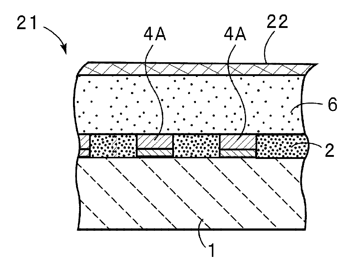
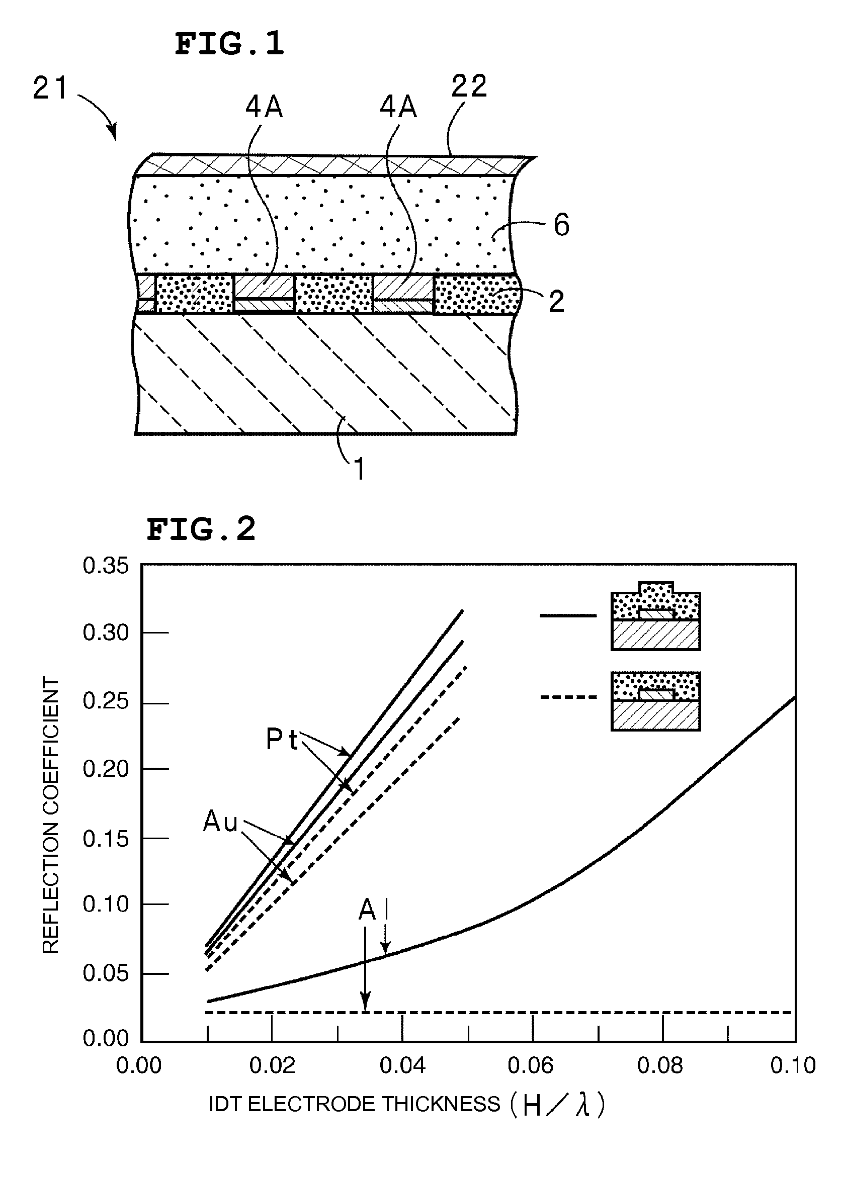
[0115]FIG. 1 is a schematic, front, cross-sectional view of a surface acoustic wave device according to a first preferred embodiment of the present invention. The electrode structure of the surface acoustic wave device of this preferred embodiment is preferably equivalent to that of the surface acoustic wave device 11 described above. That is, the electrode structure shown in FIG. 4 is also provided in the surface acoustic wave device of this preferred embodiment. Thus, FIG. 4 is also a schematic front view illustrating the electrode structure of the surface acoustic wave device of this preferred embodiment. However, in FIG. 4, a SiN layer which will be described later is omitted.

[0116]A surface acoustic wave device 21 of this preferred embodiment is formed in a similar manner to that of the above surface acoustic wave device 11 except that a SiN layer 22 is provided at the topmost portion.

[0117]That is, as shown in FIG. 1, the surface acoustic wave device 21 includes a piezoelectri...

second preferred embodiment

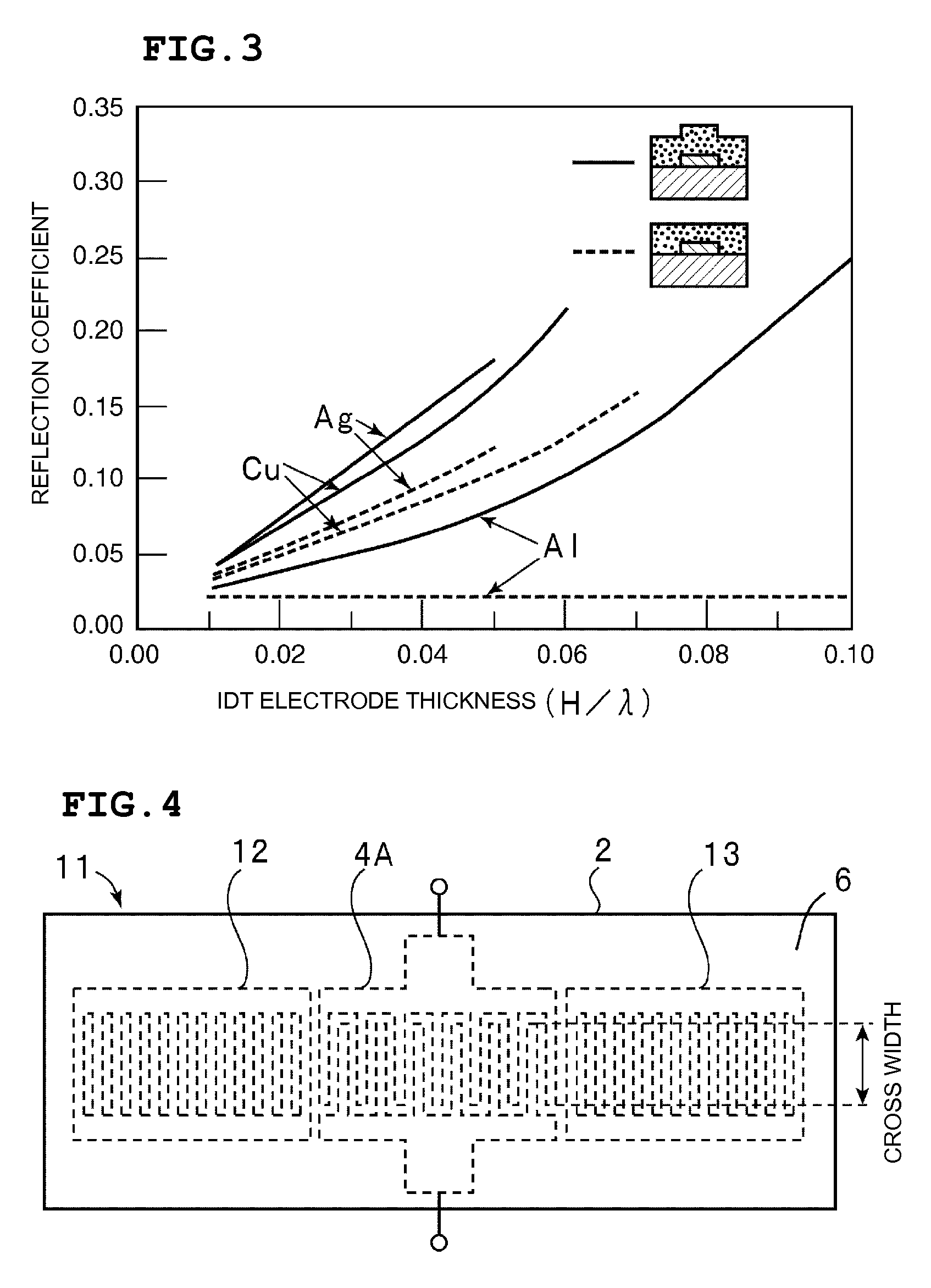
[0154]FIG. 14 is a schematic, front, cross-sectional view of a surface acoustic wave device of a second preferred embodiment according to the present invention. In a surface acoustic wave device 31, the electrode is formed on the 36° rotated Y-plate X-propagation LiTaO3 substrate 1. The electrode has a plane shape equivalent to that of the first preferred embodiment. That is, in this preferred embodiment, the electrode including the IDT electrode 4A and a pair of the reflectors 12 and 13 is arranged so as to define a one-port type surface acoustic wave device for a 1.9 GHz band.

[0155]In addition, the electrode includes a Ti film, a Cu film, and a Ti film having thicknesses of about 5 nm, about 65 nm, and about 10 nm, respectively. Then, a first SiO2 layer 32 is provided so as to have a thickness of about 80 nm.

[0156]In this preferred embodiment, a diffusion inhibition film 35 is disposed so as to cover the electrode and the first SiO2 layer 32. The diffusion inhibition film 35 is ma...


PUM

PropertyMeasurementUnit
reflection coefficientaaaaaaaaaa
Euler anglesaaaaaaaaaa

Abstract

A surface acoustic wave device includes a piezoelectric substrate made of LiTaO3 or LiNbO3 having an electromechanical coefficient of about 15% or more, at least one electrode which is disposed on the piezoelectric substrate and which is a laminate film having a metal layer defining a primary metal layer primarily composed of a metal having a density higher than that of Al or an alloy of the metal and a metal layer which is laminated on the primary metal layer and which is composed of another metal, and a first SiO2 layer which is disposed in a remaining area other than that at which the at least one electrode is located and which has a thickness approximately equivalent to that of the electrode. In the surface acoustic wave device described above, the density of the electrode is at least about 1.5 times that of the first SiO2 layer. In addition, a second SiO2 layer disposed so as to cover the electrode and the first SiO2 layer and a silicon nitride compound layer disposed on the second SiO2 layer are further provided.

Description

BACKGROUND OF THE INVENTION[0001]1. Field of the Invention[0002]The present invention relates to a surface acoustic wave device used, for example, for a resonator and a band pass filter, and more particularly, relates to a surface acoustic wave device having a structure in which an insulating layer is arranged so as to cover electrodes.[0003]2. Description of the Related Art[0004]A DPX and an RF filter used for mobile communication systems have been required to satisfy broadband properties and superior temperature properties. Heretofore, in a surface acoustic wave device used for a DPX and an RF filter, a piezoelectric substrate of 36° to 50° rotated Y-plate X-propagation LiTaO3 has been used. This piezoelectric substrate has a frequency-temperature coefficient of approximately −40 ppm / ° C. to −30 ppm / ° C. Hence, in order to improve the temperature properties, a method has been used in which a SiO2 film having a positive frequency-temperature coefficient is formed on the piezoelectr...

Claims


Application Information

Patent Timeline
Patent Type & Authority Patents(United States)
IPC IPC(8): H01L41/08H01L41/00H03H3/08H03H9/02H03H9/145H03H9/25
CPCH03H3/08H03H9/02984H03H9/14538H03H9/25
Inventor NISHIYAMA, KENJITAKATA, EIICHINAKAO, TAKESHIKADOTA, MICHIO
Owner MURATA MFG CO LTD
Why Eureka
Try Eureka