Light-emitting device, film-forming method and manufacturing apparatus thereof, and cleaning method of the manufacturing apparatus

a technology of light-emitting devices and manufacturing apparatuses, which is applied in the direction of vacuum evaporation coating, applications, and other domestic objects, to achieve the effects of reducing surface area, preventing gas discharge, and reducing drive voltag

Inactive Publication Date: 2005-01-27
SEMICON ENERGY LAB CO LTD
View PDF33 Cites 97 Cited by
  • Summary
  • Abstract
  • Description
  • Claims
  • Application Information

AI Technical Summary

Benefits of technology

[0033] In addition, in each configuration of the above-described film forming apparatus, the vacuum pumping means which is disposed so as to be coupled to the film forming chamber vacuates a level of IPa from an atmospheric pressure by an oil-free dry pump, and vacuates a pressure more than that by a magnetic levitation type turbo molecular pump or a complex molecular pump. In the film forming chamber, for the purpose of removing moisture, a cryopump may be disposed in parallel. By doing this, contamination due to an organic matter such as mainly, oil is prevented from pumping means. An inner wall surface is processed as a mirror surface by electrolytic polishing, and a surface area is reduced so that gas discharge is prevented.
[0034] In addition, in the above-described each film forming apparatus, by disposing a plurality of deposition sources in one film forming chamber, it is possible to form a plurality of functional regions, and a light emitting device which has a mixed regio

Problems solved by technology

Further, it has, as a problem, providing a film fo

Method used


Image

  • Light-emitting device, film-forming method and manufacturing apparatus thereof, and cleaning method of the manufacturing apparatus
  • Light-emitting device, film-forming method and manufacturing apparatus thereof, and cleaning method of the manufacturing apparatus
  • Light-emitting device, film-forming method and manufacturing apparatus thereof, and cleaning method of the manufacturing apparatus

Examples


embodiment mode 1

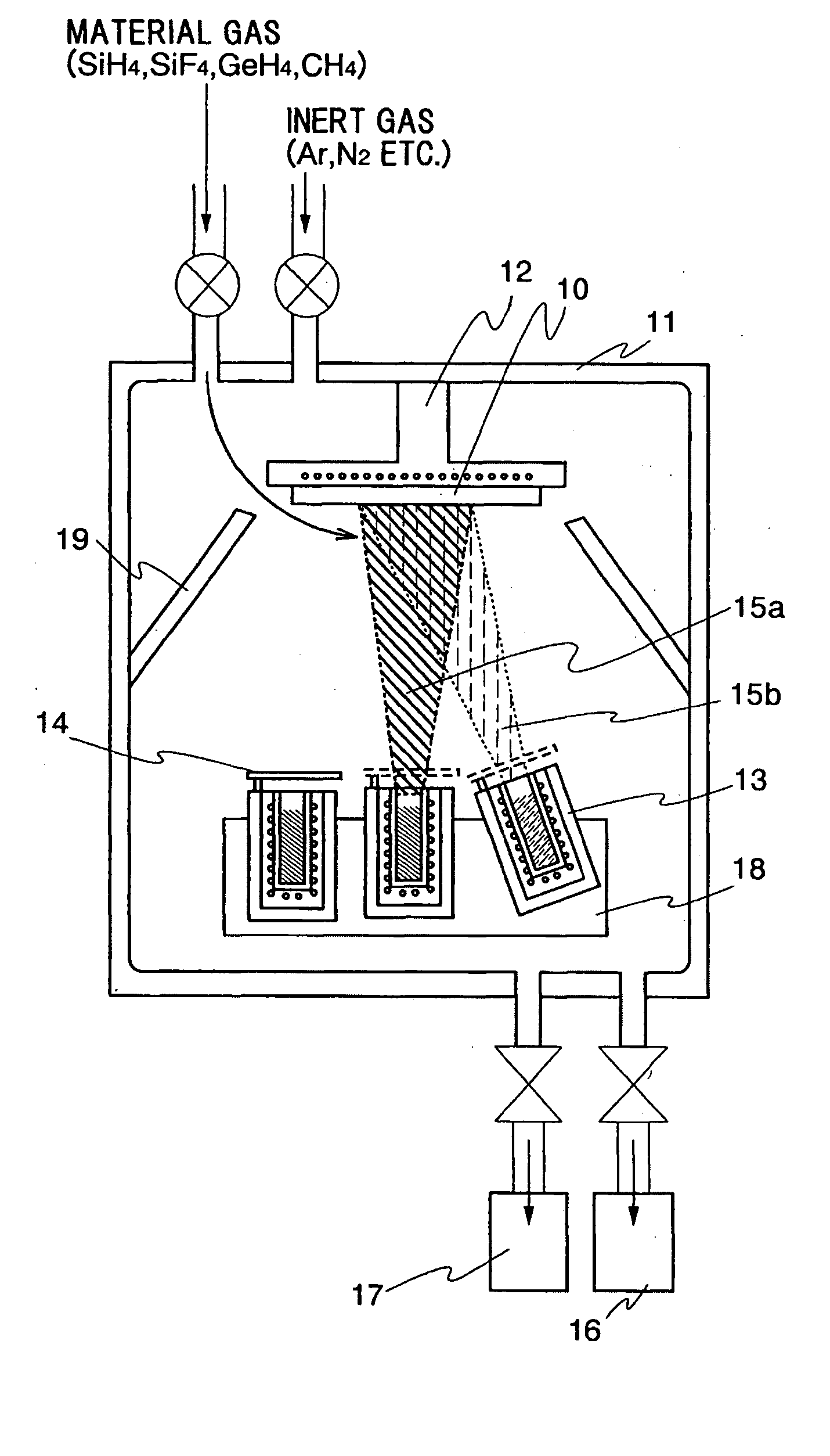
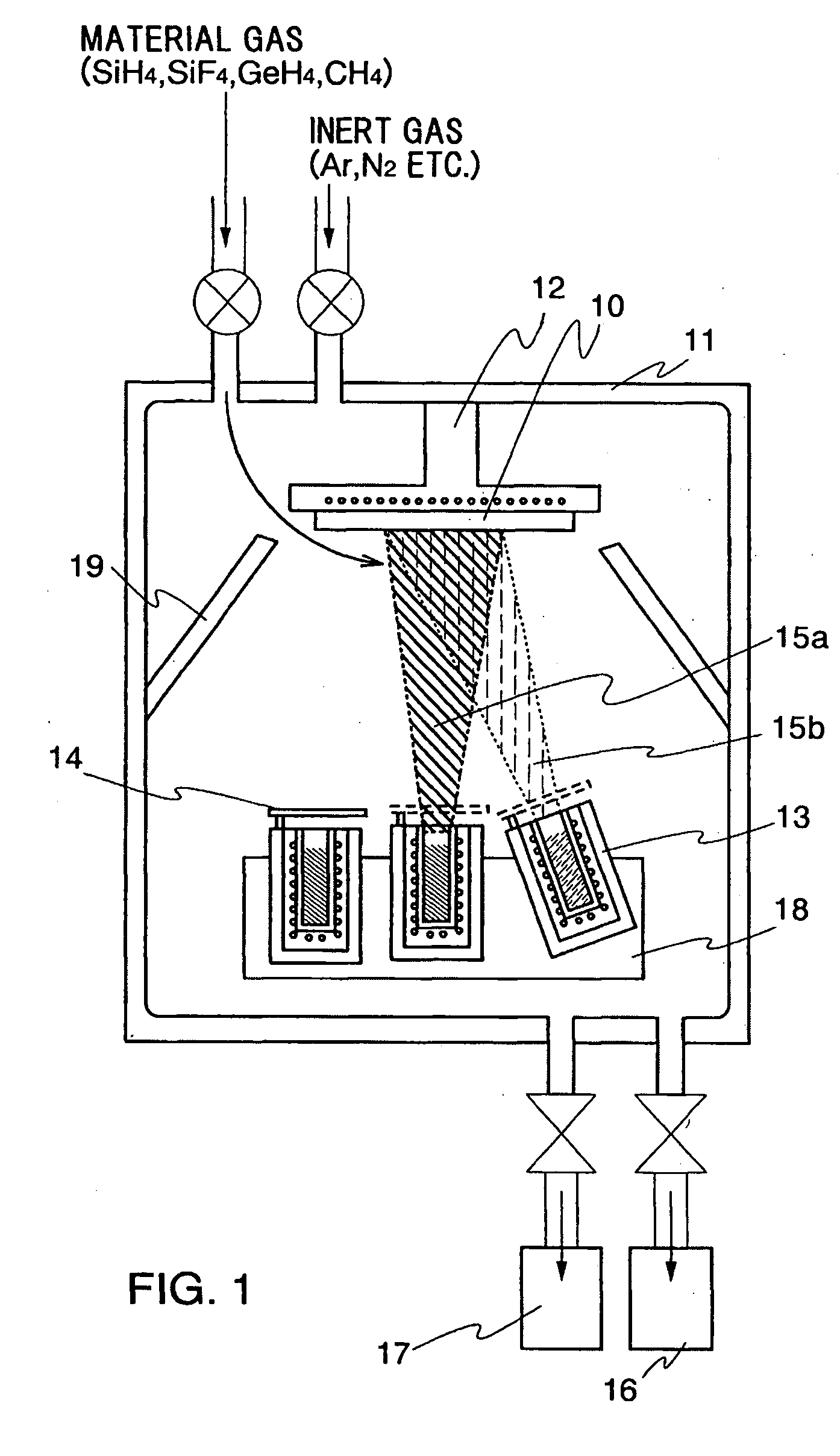
[0065] A configuration of a film forming apparatus in this invention will be described by use of FIG. 1. FIG. 1 is one example of a cross-sectional view in the film forming apparatus of this invention.

[0066] On the occasion of carrying out film formation by a deposition method, it is preferable to use a face-down system (also called as a depo-up system), and a substrate 10 is set with a film formed surface downward. A system, in which film formation is carried out with a film formed surface of a substrate face downward, is called as the face-down system, and according to this system, it is possible to suppress attachment of dust.

[0067] As shown in FIG. 1, in contact with the substrate 10, heating means, here, a heater is disposed on a substrate holder 12. By heating means, it is possible to set temperature of the substrate to 50-200° C., preferably, 65-150° C. In addition, the substrate 10 is fixed by being sandwiched by metal masks (not shown in the figure), by a permanent magnet...

embodiment mode 2

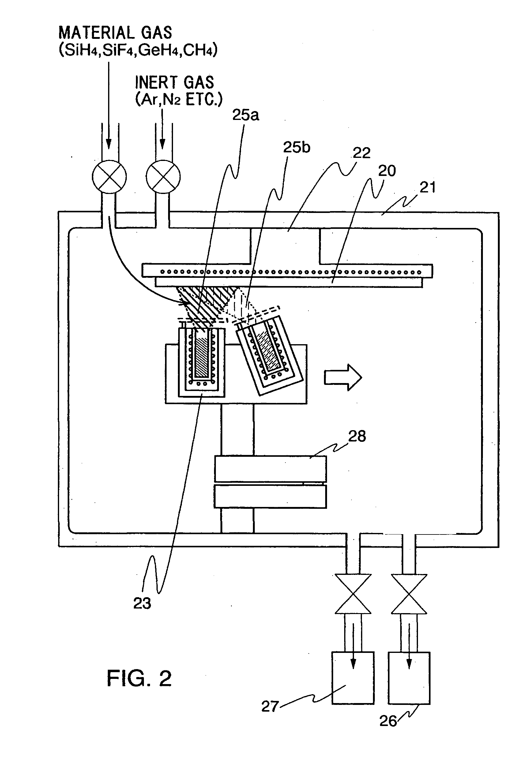
[0096] Here, a film forming apparatus, which is different from the embodiment mode 1, is shown in FIG. 2.

[0097]FIG. 2 shows an example of a film forming apparatus in which a deposition source is moved (or rotated), so as for a film to be formed uniformly.

[0098] In FIG. 2, 20 designates a substrate, and 21 designates a chamber wall, and 22 designates a substrate holder, and 23 designates a cell, and 25a designates an evaporated first material, and 25b designates an evaporated second material, and 26 designates a turbo molecular pump, and 27 designates a cryopump, and 28 designates a moving mechanism for moving the cell. Since there is no necessity to rotate the substrate, it is possible to provide a deposition apparatus which can correspond to a large area substrate. In addition, by the deposition cell 23 moving in a X axis direction and a Y axis direction to the substrate, it becomes possible to form a deposition film uniformly.

[0099] In the deposition apparatus of this invention...

embodiment mode 3

[0106] Here, a film forming apparatus, which is different from the embodiment mode 1, is shown in FIG. 3. In passing, the same reference numerals are used for the same places as in FIG. 1.

[0107] The film forming apparatus shown in FIG. 3 is an example in which deposition is carried out over introducing material gas, which was radicalized by plasma generating means in advance, into a film forming chamber.

[0108] As shown in FIG. 3, a microwave source 30a is connected to a waveguide 30b. This waveguide 30b forms plasma 30c due to glow discharge, by carrying out irradiation to material gas in a discharge tube. From the microwave source which is used here, μ wave of approximately 2.45 GHz is radiated.

[0109] For example, in case that monosilane gas was used as material gas, an oxide silicon precursor such as SiHx, SiHxOy, SiOy is generated, and introduced into a film forming chamber. These radicals are easily reacted with oxygen and moisture, and it is possible to reduce oxygen concent...


PUM

PropertyMeasurementUnit
Pressureaaaaaaaaaa

Abstract

This invention provides a new film forming method in which, on the occasion that pressure is decreased by pressure decreasing means which was connected to a film forming chamber, and a film is formed by evaporating an organic compound material from a deposition source in the film forming chamber, minute amounts of gas (silane series gas) which comprises smaller particles than particles of the organic compound material, i.e., a material with a smaller atomic radius are flowed, and the material with a small atomic radius is made to be included in an organic compound film.

Description

TECHNICAL FIELD [0001] This invention relates a film forming apparatus, a manufacturing apparatus, a cleaning method, and a film forming method, which are used for film formation of a material which can be formed as a film by deposition (hereinafter, referred to as a deposition material). In particular, this invention is a technology which is effective in case of using a material which includes an organic compound, as a deposition material. BACKGROUND ART [0002] In recent years, research of a light emitting apparatus which used an EL device as a self-luminous type device has been intensified, and in particular, a light emitting apparatus which used an organic material as the EL material has been attracting attention. This light emitting apparatus is also called as an organic EL display or an organic light emitting diode. [0003] A light emitting apparatus has such a characteristic that there is no problem of a view field angle since it is of a self-luminous type, unlike a liquid crys...

Claims


Application Information

Patent Timeline
IPC IPC(8): C23C14/12C23C14/24C23C14/56C23C14/58H01L51/00H01L51/30H01L51/40H01L51/56H05B33/10
CPCC23C14/12Y10S428/917C23C14/246C23C14/564C23C14/5806H01L51/001H01L51/002H01L51/0037H01L51/0059H01L51/0062H01L51/007H01L51/0077H01L51/0078H01L51/0081H01L51/0085H01L51/56H05B33/10C23C14/24H10K71/164H10K71/30H10K85/1135H10K85/649H10K85/631H10K85/6565H10K85/311H10K85/30H10K85/324H10K85/342H10K71/00
Inventor YAMAZAKI, SHUNPEI
Owner SEMICON ENERGY LAB CO LTD
Why Eureka
Try Eureka