Process for realizing a connecting structure

a technology of connecting structure and process, which is applied in the direction of semiconductor devices, semiconductor/solid-state device details, electrical apparatus, etc., can solve the problems of limiting the application of such techniques, limiting the manufacturing limit of classic semiconductor technology, and difficult to achieve perfect alignment as shown in fig. 8b, so as to prevent the dispersion of metal composing the connecting structure

Active Publication Date: 2015-12-29
SONY SEMICON SOLUTIONS CORP
View PDF16 Cites 101 Cited by
  • Summary
  • Abstract
  • Description
  • Claims
  • Application Information

AI Technical Summary

Benefits of technology

[0011]Accordingly, the present invention now provides a connecting structure to be used in a semiconductor substrate subjected to 3D integration such that diffusion of the metal composing the connecting structure is prevented, even in the presence of a misalignment during the 3D integration process.
[0012]In particular, the present invention relates to a process for realizing a connecting structure in a semiconductor substrate, according to an embodiment of the present invention, the semiconductor substrate having at least a first surface, and being foreseen for a 3D integration with a second substrate along the first surface, wherein the 3D integration is subject to a lateral misalignment in at least one dimension having a misalignment value (M), can include the step of growing a diffusion barrier structure for preventing diffusion of elements out of a conductive layer into the rest of the semiconductor substrate, is characterized in that a first end surface, being the most outward surface of the diffusion barrier structure being substantially parallel to the first surface, along a direction perpendicular to the first surface and going from the substrate toward the first surface, of the diffusion barrier structure can have a length, in the direction of the lateral misalignment, the length being dependent on the misalignment value, wherein the length of the diffusion barrier structure is chosen such that in a 3D integrated structure a diffusion of elements out of a conductive layer of the second substrate is prevented in the integrated state.
[0013]By carrying out such process, it is possible to realize a connecting structure which can be aligned during a 3D integration process, to a corresponding connecting structure on the first integrated substrate, even in the presence of a misalignment during the 3D integration. By taking into account the misalignment value, the diffusion barrier structure can be sized so as to compensate for the misalignment and prevent diffusion of a conductive element.

Problems solved by technology

As standard semiconductor manufacturing techniques are pushed toward shorter gate length, they approach the manufacturing limit of classic semiconductor technology.
Due to technological limits, however, a perfect alignment as shown in FIG. 8B can be hard to achieve.
This problem is present in current 3D integration techniques and can therefore prevent or limit the application of such techniques in industrial manufacturing of integrated systems.

Method used


Image

  • Process for realizing a connecting structure
  • Process for realizing a connecting structure
  • Process for realizing a connecting structure

Examples


first embodiment

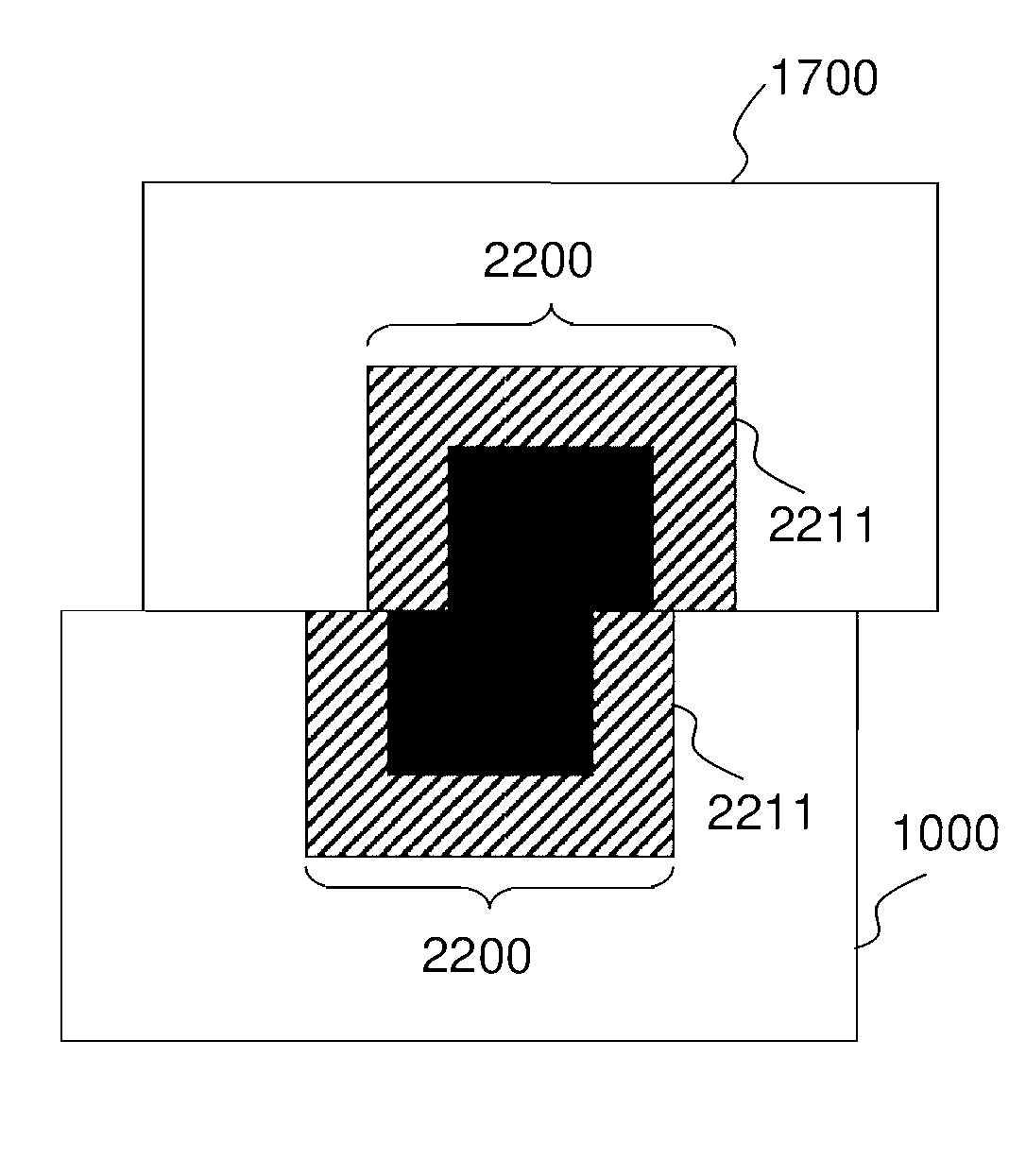
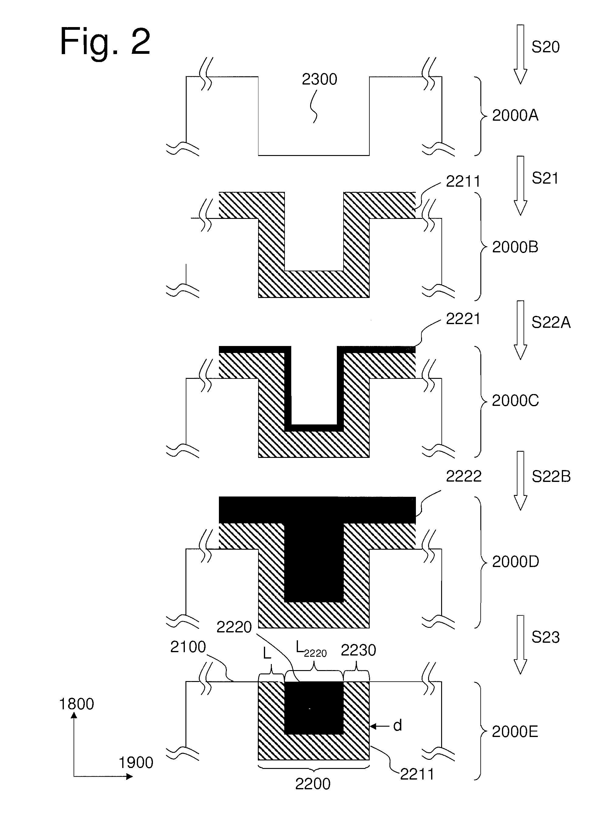
[0071]FIG. 2 is a schematic drawing illustrating a process for realizing a connecting structure according to the present invention. More specifically, FIG. 2 illustrates a process of realizing a connecting structure 2200 such as connecting structure 1201 of the first semiconductor substrate 1000, and / or connecting structure 1202 of the second semiconductor substrate 1700, and / or any of connecting structures 1200 of FIG. 1.

[0072]A semiconductor substrate 2000A includes a hole 2300, as can be seen in FIG. 2. The hole 2300 might be realized starting from a semiconductor substrate through step S20, by carrying out, for instance, photolithography and etching. The size, shape, depth and position of hole 2300 might be controlled in a manner known in the art of semiconductor manufacturing.

[0073]By carrying out a deposition and / or growing step S21, a diffusion barrier layer 2211 is realized on top of semiconductor substrate 2000A so as to obtain semiconductor substrate 2000B. The realization...

second embodiment

[0089]FIG. 4 is a schematic drawing illustrating a process for realizing a connecting structure 4200 according to the present invention. More specifically, FIG. 4 illustrates a process of realizing a connecting structure 4200 such as connecting structure 1201 of the first semiconductor substrate 1000, and / or connecting structure 1202 of the second semiconductor substrate 1700, and / or any of connecting structures 1200 of FIG. 1.

[0090]As can be seen in FIG. 4, a semiconductor substrate 4000A having a first hole 4320 and a second hole 4310 encircling the first hole toward the surface 4100 could be obtained by a step S40. The first hole 4320 might be realized starting from a semiconductor substrate through step S40, by carrying out, for instance, photolithography and etching. The size, shape, depth and position of first hole 4320 might be controlled in a manner known in the art of semiconductor manufacturing. Similarly, the second hole 4310 might be realized starting from a bulk semicon...

third embodiment

[0097]FIG. 5 is a schematic drawing illustrating a process for realizing a connecting structure 5200 according to the present invention. More specifically, FIG. 5 illustrates a process of realizing a connecting structure 5200 such as connecting structure 1201 of the first semiconductor substrate 1000, and / or connecting structure 1202 of the second semiconductor substrate 1700, and / or any of connecting structures 1200 of FIG. 1.

[0098]FIG. 5 illustrates a semiconductor substrate 5000A with a conductive layer 5220 and a diffusion barrier layer 5212 achieved by a step S52. Techniques for carrying out step S52 could be substantially similar to techniques for carrying out steps S22A and S22B in FIG. 2.

[0099]Subsequently, a semiconductor substrate 5000B having a hole 5310 on the diffusion barrier layer 5212 surrounding the conductive layer 5220 or near the surface 5100 is obtained by a step S50. The size, shape, depth and position of hole 5310 might be controlled in a manner known in the a...


PUM


Abstract

The present invention relates to a process for realizing a connecting structure in a semiconductor substrate, and the semiconductor substrate realized accordingly. The semiconductor substrate has at least a first surface, and is foreseen for a 3D integration with a second substrate along the first surface, wherein the 3D integration is subject to a lateral misalignment in at least one dimension having a misalignment value. This process includes growing a diffusion barrier structure for preventing diffusion of elements out of a conductive layer into the rest of the semiconductor substrate, wherein a first end surface, being the most outward surface of the diffusion barrier structure and being substantially parallel to the first surface, along a direction perpendicular to the first surface and going from the substrate toward the first surface, of the diffusion barrier structure can have a length, in the direction of the lateral misalignment, the length being dependent on the misalignment value, wherein the length of the diffusion barrier structure is chosen such that in a 3D integrated structure a diffusion of elements out of a conductive layer of the second substrate is prevented in the integrated state.

Description

TECHNICAL FIELD[0001]The present invention relates to a process for realizing a connecting structure in a semiconductor substrate and a semiconductor system including a semiconductor substrate in which such a connecting structure has been realized.BACKGROUND[0002]As standard semiconductor manufacturing techniques are pushed toward shorter gate length, they approach the manufacturing limit of classic semiconductor technology. In order to further improve performances, reduce power consumption and packaging costs, integration techniques, such as 3D integration are becoming more and more common.[0003]3D integration consists in connecting at least two modules such as a semiconductor die, an optical module, a heat dissipation module, a biological module, and a memory, by stacking them one upon each other. Such an approach has several advantages. PCB-requirements are more relaxed since the integration is performed on a vertical direction. Power consumption of the input / output interfaces as...

Claims


Application Information

Patent Timeline
Patent Type & Authority Patents(United States)
IPC IPC(8): H01L23/48H01L23/52H01L29/40H01L21/30H01L21/46H01L23/00H01L25/065H01L25/00
CPCH01L24/05H01L24/03H01L25/0657H01L25/50H01L24/80H01L24/94H01L2224/034H01L2224/0332H01L2224/0345H01L2224/03452H01L2224/03462H01L2224/03616H01L2224/05006H01L2224/05082H01L2224/05139H01L2224/05144H01L2224/05147H01L2224/05181H01L2224/05186H01L2224/05187H01L2224/05546H01L2224/05547H01L2224/05576H01L2224/05578H01L2224/05639H01L2224/05644H01L2224/05647H01L2224/05681H01L2224/05687H01L2224/08121H01L2224/80203H01L2224/80357H01L2224/80895H01L2225/06513H01L2924/0105H01L2924/01005H01L2924/01006H01L2924/01013H01L2924/01014H01L2924/01029H01L2924/01032H01L2924/01033H01L2924/01047H01L2924/01073H01L2924/01075H01L2924/01079H01L2924/10329H01L2924/15788H01L2924/00014H01L2924/04953H01L2924/05042H01L2924/04941H01L2924/00H01L2224/02126H01L2924/14H01L21/48H01L23/12
Inventor LANDRU, DIDIER
Owner SONY SEMICON SOLUTIONS CORP
Why Eureka
Try Eureka