

How to form a mos transistor
A MOS transistor and layer-forming technology, applied in semiconductor devices, electrical components, circuits, etc., can solve the problems of MOS transistor carrier mobility decrease, device performance impact, etc., to prevent metal diffusion, improve performance, and save time. Effect
- Summary
- Abstract
- Description
- Claims
- Application Information
AI Technical Summary
Problems solved by technology
Method used
Image

Examples
Embodiment Construction
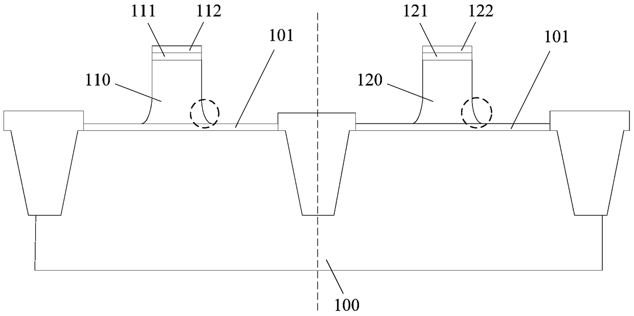
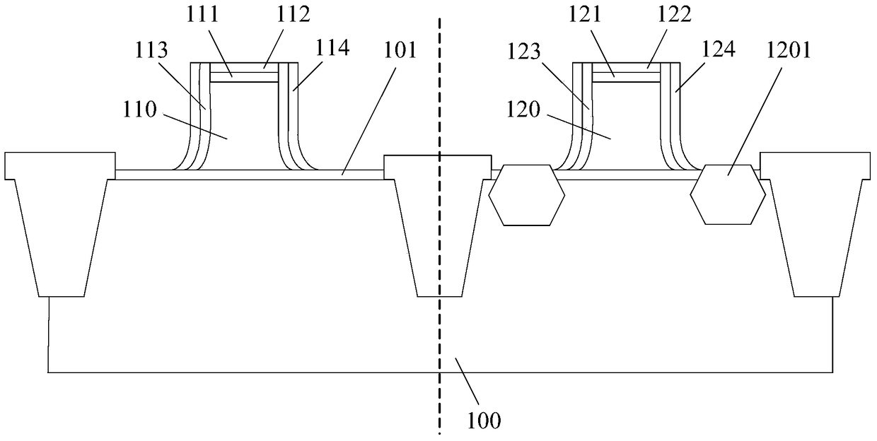
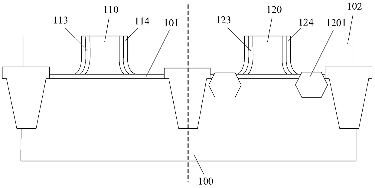
[0031] The inventors found that the aluminum in the metal gate has two diffusion routes, one is to diffuse downward through the bottom of the metal aluminum gate (that is, it diffuses downward through the top of the channel region), and the other is to diffuse through both sides of the metal aluminum gate. diffusion. Although, in the existing MOS transistor formation method, a diffusion barrier layer is first formed in the groove for filling the metal gate before making the metal gate to prevent aluminum from diffusing, however, the diffusion barrier layer produced by the existing method usually There will be a large shrinkage stress (especially the diffusion barrier layer formed by physical vapor deposition method, the stress is relatively large), under the action of stress, the diffusion barrier layer will appear thick at the center of the bottom of the groove, and the two sides of the groove will be thick. In the case where the thickness of the side bottom corner part gradu...
PUM
 Abstract
Description
Claims
Application Information